Pixel circuit, driving method thereof, and active matrix organic light emitting display

A technology of pixel circuit and power supply, applied in the field of flat panel display, can solve the problems of poor display uniformity and the existence of micro-bright spots, and achieve the effects of improving contrast, weakening micro-bright spots, and improving display uniformity

Active Publication Date: 2017-07-11
CHENGDU VISTAR OPTEOLECTRONICS CO LTD
View PDF5 Cites 0 Cited by
  • Summary
  • Abstract
  • Description
  • Claims
  • Application Information

AI Technical Summary

Problems solved by technology

[0008] The object of the present invention is to provide a pixel circuit and its driving method and an active matrix organic light emitting display to solve the problems of poor display uniformity and micro bright spots in the existing active matrix organic light emitting display

Method used


Image

  • Pixel circuit, driving method thereof, and active matrix organic light emitting display
  • Pixel circuit, driving method thereof, and active matrix organic light emitting display
  • Pixel circuit, driving method thereof, and active matrix organic light emitting display

Examples


Embodiment 1

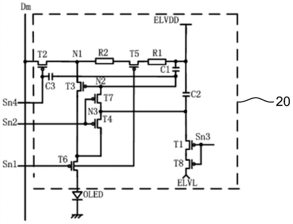
[0040] Please refer to figure 2 , which is a schematic structural diagram of a pixel circuit according to Embodiment 1 of the present invention. Such as figure 2As shown, the pixel circuit 20 includes: a first thin film transistor T1 connected between the third node N3 and the third power supply ELVL, the gate of which is connected to the third scan line Sn3; a second thin film transistor T2 connected to the data Between the line Dm and the first node N1, its gate is connected to the fourth scanning line Sn4; the third thin film transistor T3 is connected between the first node N1 and the source of the sixth thin film transistor T6, and its gate is connected to The second node N2; the fourth thin film transistor T4, connected between the third node N3 and the source of the sixth thin film transistor T6, the gate of which is connected to the second scanning line Sn2; the fifth thin film transistor T5, connected to the first Between the power supply ELVDD and the first node ...

Embodiment 2

[0063] Please refer to Figure 4 , which is a schematic structural diagram of a pixel circuit according to Embodiment 2 of the present invention. Such as Figure 4As shown, the pixel circuit 30 includes: a first thin film transistor T1 connected between the third node N3 and the third power supply ELVL, the gate of which is connected to the third scan line Sn3; a second thin film transistor T2 connected to the data Between the line Dm and the first node N1, its gate is connected to the fourth scanning line Sn4; the third thin film transistor T3 is connected between the first node N1 and the source of the sixth thin film transistor T6, and its gate is connected to The second node N2; the fourth thin film transistor T4, connected between the third node N3 and the source of the sixth thin film transistor T6, the gate of which is connected to the second scanning line Sn2; the fifth thin film transistor T5, connected to the first Between the power supply ELVDD and the first node ...

Embodiment 3

[0067] Please refer to Figure 5 , which is a schematic structural diagram of a pixel circuit according to Embodiment 3 of the present invention. Such as Figure 5 As shown, the pixel circuit 40 includes: a first thin film transistor T1 connected between the third node N3 and the third power supply ELVL, the gate of which is connected to the third scan line Sn3; a second thin film transistor T2 connected to the data Between the line Dm and the first node N1, its gate is connected to the fourth scanning line Sn4; the third thin film transistor T3 is connected between the first node N1 and the source of the sixth thin film transistor T6, and its gate is connected to The second node N2; the fourth thin film transistor T4, connected between the third node N3 and the source of the sixth thin film transistor T6, the gate of which is connected to the second scanning line Sn2; the fifth thin film transistor T5, connected to the first Between the power supply ELVDD and the first node...


PUM


Abstract

In the pixel circuit and its driving method and the active matrix organic light-emitting display provided by the present invention, by adding a series resistor in the pixel circuit, the influence of the voltage drop of the power line and the leakage current on the display effect is reduced, thereby improving the display uniformity, and The leakage current path of the pixel circuit is only one, and the leakage current path is composed of a plurality of thin film transistors in series, which can further reduce the leakage current, thus, the organic light-emitting display using the pixel circuit and its driving method can not only reduce the The micro-bright spots in the dark state can improve the contrast, and can also improve the display uniformity.

Description

technical field [0001] The invention relates to the technical field of flat panel display, in particular to a pixel circuit, a driving method thereof, and an active matrix organic light emitting display. Background technique [0002] Active Matrix Organic Light Emitting Display (English full name Active Matrix Organic Lighting Emitting Display, referred to as AMOLED) can emit light by itself, unlike thin film transistor liquid crystal display (English full name Thin Film Transistor liquid crystal display, referred to as TFT-LCD) requires a backlight system (backlight system) It can be lighted, so the visibility and brightness are higher, and it is thinner and lighter. At present, active matrix organic light-emitting displays are hailed as a new generation of displays that can replace thin-film transistor liquid crystal displays. [0003] In an active matrix organic light emitting display, each pixel includes an organic light emitting diode (English full name Organic Lightin...

Claims


Application Information

Patent Timeline
Patent Type & Authority Patents(China)
IPC IPC(8): G09G3/3233
Inventor 朱晖胡思明张婷婷杨楠刘周英张小宝
Owner CHENGDU VISTAR OPTEOLECTRONICS CO LTD
Why Eureka
Try Eureka