Method for preparing all-dielectric ultra-thin two-dimensional circular polarization dichroic device

一种二维圆、全介质的技术,应用在偏振元件、仪器、光学元件等方向,能够解决透过率能量上区分度小、结构区分度低、作用波段窄等问题,达到时间成本低、原料来源广、易于制作的效果

Active Publication Date: 2018-11-27
SUZHOU UNIV
View PDF3 Cites 0 Cited by
  • Summary
  • Abstract
  • Description
  • Claims
  • Application Information

AI Technical Summary

Problems solved by technology

However, this structure can only distinguish left and right circularly polarized light in terms of mode, and the degree of discrimination in transmittance energy is extremely small.
The existing technology has disadvantages such as low structural discrimination, narrow action band, and incompatibility with traditional semiconductor processes.

Method used


Image

  • Method for preparing all-dielectric ultra-thin two-dimensional circular polarization dichroic device
  • Method for preparing all-dielectric ultra-thin two-dimensional circular polarization dichroic device
  • Method for preparing all-dielectric ultra-thin two-dimensional circular polarization dichroic device

Examples


Embodiment 1

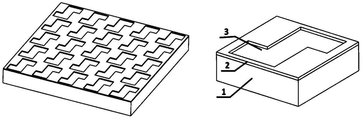
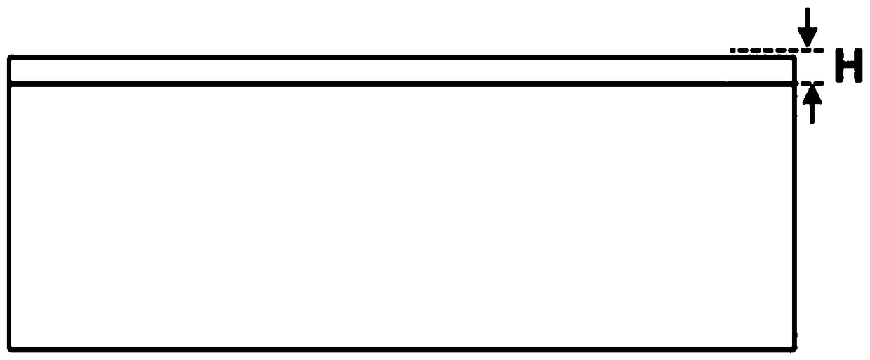
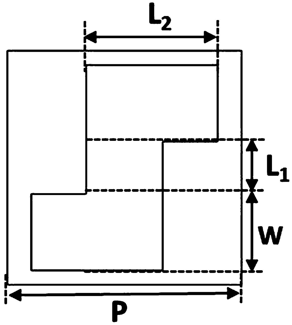
[0031] See attached figure 2 , is a schematic diagram of the front-view structure of the structural unit of an all-dielectric ultra-thin two-dimensional circular polarization dichroic device, wherein the thickness H of silicon in the semiconductor dielectric layer is 0.25 μm; see the attached image 3 , is a top view structure diagram of an all-dielectric ultra-thin two-dimensional circularly polarized dichroic device, in which the longitudinal arm length L1 of the Z-shaped through hole etched in the dielectric layer is 0.2 μm, the transverse arm length L2 is 0.5 μm, and the slit width W is 0.32 μm, and the period P of each structural unit is 0.98 μm.

[0032] attached Figure 4 It is the transmittance curve of left and right circularly polarized light incident through the above-mentioned all-dielectric ultra-thin two-dimensional circularly polarized dichroic device from the silica substrate; attached Figure 5 It is the circular dichroism curve of the all-dielectric ultrat...

Embodiment 2

[0039] In this embodiment, the substrate is silicon dioxide, the semiconductor dielectric layer is silicon; the thickness of the semiconductor dielectric layer is H=0.23 μm, the longitudinal arm length L1 of the Z-shaped through hole is 0.2 μm, and the lateral arm length L2 is 0.5 μm. The width is 0.32 μm, and the period of each structural unit is 0.98 μm. After the semiconductor medium layer is grown by chemical vapor deposition, the circularly polarized polarizer is directly obtained by using a focused ion beam etching process.

[0040] attached Figure 6 It is the transmittance curve of left and right circularly polarized light incident through the above-mentioned all-dielectric ultra-thin two-dimensional circularly polarized dichroic device from the silica substrate; attached Figure 7 It is the circular dichroism curve of the all-dielectric ultrathin two-dimensional circular polarization device. see Figure 6 As shown, there is a large difference in the transmittance o...

Embodiment 3

[0042] The preparation process of this embodiment is consistent with that of Embodiment 1, wherein the substrate is silicon dioxide, and the semiconductor dielectric layer is gallium arsenide; the longitudinal arm length L1 of the Z-shaped through hole is 0.2 μm, and the lateral arm length L2 is 0.5 μm. The slit width is 0.32 μm, and the thickness H of the dielectric layer is 0.25 μm. The period of each structural unit is 0.98 μm.

[0043] attached Figure 8 It is the transmittance curve of left and right circularly polarized light incident through the above-mentioned all-dielectric ultra-thin two-dimensional circularly polarized dichroic device from the silica substrate; attached Figure 9 It is the circular dichroism curve of the all-dielectric ultrathin two-dimensional circular polarization device. see Figure 8 As shown, there is a large difference in the transmittance of the structure to the left and right circularly polarized light in the 1.46μm-1.56μm band. see Fi...


PUM


Abstract

The invention provides a method for preparing an all-dielectric ultra-thin two-dimensional circular polarization dichroic device, being able to realize the effect of directly generating circularly polarized light and distinguishing left and right rotary circularly polarized light. The structure includes a substrate and Z type through holes which are covered on the substrate and etched in a dielectric layer. The polarizer of the all-dielectric ultra-thin two-dimensional circular polarization dichroic device has an average circular dichroism of more than 70% in the 1.50 mu m to 1.61 mu m wave band, can reach a maximum circular dichroism to 98.3% at 1.53 mu m, and has characteristics of being wider in the wave band, being simple in structure and being easy to manufacture feature, and having agreat application value in future optical sensing systems, advanced nanophotonic devices and integrated optical systems.

Description

[0001] The present invention belongs to the divisional application of the invention titled all-dielectric ultra-thin two-dimensional circularly polarized dichroic device and its preparation method, the application number is 201610469385.5, and the application date is June 25, 2016, and belongs to the technical part of the preparation method. technical field [0002] The invention relates to the preparation technology of optical elements, in particular to a preparation method of an all-dielectric ultra-thin two-dimensional circular polarization dichroic device. Background technique [0003] In imaging technology, because polarization imaging technology can perform long-distance image acquisition operations in harsh environments, it has absolute advantages in suppressing background noise, improving detection distance, obtaining detailed features, and identifying target camouflage. Therefore, it has a very wide range of applications, for example: it can detect hidden or camoufla...

Claims


Application Information

Patent Timeline
Patent Type & Authority Applications(China)
IPC IPC(8): G02B5/30
CPCG02B5/3025
Inventor 胡敬佩王钦华赵效楠朱爱娇林雨曹冰
Owner SUZHOU UNIV
Why Eureka
Try Eureka