All-dielectric ultra-thin two-dimensional circularly polarized dichroic device and its preparation method

A two-dimensional circular, all-dielectric technology, applied in the direction of polarizing elements, instruments, optical elements, etc., can solve the problems of small transmittance energy discrimination, low structural discrimination, narrow action band, etc., to achieve low time cost, The effect of wide source of raw materials and easy production

Active Publication Date: 2018-07-20
JIANGSU INST OF ADVANCED SEMICON CO LTD
View PDF4 Cites 0 Cited by
  • Summary
  • Abstract
  • Description
  • Claims
  • Application Information

AI Technical Summary

Problems solved by technology

However, this structure can only distinguish left and right circularly polarized light in terms of mode, and the degree of discrimination in transmittance energy is extremely small.
The existing technology has disadvantages such as low structural discrimination, narrow action band, and incompatibility with traditional semiconductor processes.

Method used


Image

  • All-dielectric ultra-thin two-dimensional circularly polarized dichroic device and its preparation method
  • All-dielectric ultra-thin two-dimensional circularly polarized dichroic device and its preparation method
  • All-dielectric ultra-thin two-dimensional circularly polarized dichroic device and its preparation method

Examples


Embodiment 1

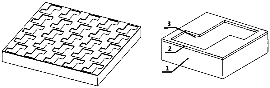
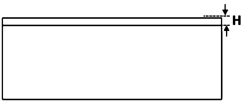
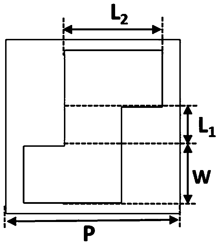
[0030] See attached figure 2 , is a schematic diagram of the front-view structure of the structural unit of an all-dielectric ultra-thin two-dimensional circular polarization dichroic device, wherein the thickness H of silicon in the semiconductor dielectric layer is 0.25 μm; see the attached image 3 , is a top view structure diagram of an all-dielectric ultra-thin two-dimensional circularly polarized dichroic device, in which the longitudinal arm length L1 of the Z-shaped through hole etched in the dielectric layer is 0.2 μm, the transverse arm length L2 is 0.5 μm, and the slit width W is 0.32 μm, and the period P of each structural unit is 0.98 μm.

[0031] attached Figure 4 It is the transmittance curve of left and right circularly polarized light incident through the above-mentioned all-dielectric ultra-thin two-dimensional circularly polarized dichroic device from the silica substrate; attached Figure 5 It is the circular dichroism curve of the all-dielectric ultrat...

Embodiment 2

[0038] In this embodiment, the substrate is silicon dioxide, the semiconductor dielectric layer is silicon; the thickness of the semiconductor dielectric layer is H=0.23 μm, the longitudinal arm length L1 of the Z-shaped through hole is 0.2 μm, and the lateral arm length L2 is 0.5 μm. The width is 0.32 μm, and the period of each structural unit is 0.98 μm. After the semiconductor medium layer is grown by chemical vapor deposition, the circularly polarized polarizer is directly obtained by using a focused ion beam etching process.

[0039] attached Figure 6 It is the transmittance curve of left and right circularly polarized light incident through the above-mentioned all-dielectric ultra-thin two-dimensional circularly polarized dichroic device from the silica substrate; attached Figure 7 It is the circular dichroism curve of the all-dielectric ultrathin two-dimensional circular polarization device. see Figure 6 As shown, there is a large difference in the transmittance o...

Embodiment 3

[0041] The preparation process of this embodiment is consistent with that of Embodiment 1, wherein the substrate is silicon dioxide, and the semiconductor dielectric layer is gallium arsenide; the longitudinal arm length L1 of the Z-shaped through hole is 0.2 μm, and the lateral arm length L2 is 0.5 μm. The slit width is 0.32 μm, and the thickness H of the dielectric layer is 0.25 μm. The period of each structural unit is 0.98 μm.

[0042] attached Figure 8 It is the transmittance curve of left and right circularly polarized light incident through the above-mentioned all-dielectric ultra-thin two-dimensional circularly polarized dichroic device from the silica substrate; attached Figure 9 It is the circular dichroism curve of the all-dielectric ultrathin two-dimensional circular polarization device. see Figure 8 As shown, there is a large difference in the transmittance of the structure to the left and right circularly polarized light in the 1.46μm-1.56μm band. see Fi...


PUM


Abstract

The invention provides an all-dielectric ultra-thin two-dimensional circular polarization dichroic device and a preparation method thereof, which can realize the functions of directly generating circularly polarized light and distinguishing left and right circularly polarized light. The structure includes a substrate and a Z-shaped through hole etched in the dielectric layer covering the substrate; the polarizer of the present invention has an average circular dichroism of more than 70% in the 1.50μm-1.61μm band, and a circular dichroism at 1.53μm. The highest dichroism can reach 98.3%, and it has the characteristics of wide wavelength band, simple structure and easy fabrication. It has great application value in future optical sensing systems, advanced nanophotonic devices and integrated optical systems.

Description

technical field [0001] The invention relates to the preparation technology of optical elements, in particular to the design and preparation method of an all-dielectric ultra-thin two-dimensional circular polarization dichroic device. Background technique [0002] In imaging technology, because polarization imaging technology can perform long-distance image acquisition operations in harsh environments, it has absolute advantages in suppressing background noise, improving detection distance, obtaining detailed features, and identifying target camouflage. Therefore, it has a very wide range of applications, for example: it can detect hidden or camouflaged targets; it can realize the detection and identification of sea surface and underwater targets; it can realize navigation under smoky weather conditions; It can distinguish real targets in objects; it can perform medical diagnosis such as cancer and burns; it can identify object characteristics (such as fingerprints, etc.); it...

Claims


Application Information

Patent Timeline
Patent Type & Authority Patents(China)
IPC IPC(8): G02B5/30
CPCG02B5/3025
Inventor 胡敬佩王钦华赵效楠朱爱娇林雨曹冰
Owner JIANGSU INST OF ADVANCED SEMICON CO LTD
Why Eureka
Try Eureka