
GOA circuit

A circuit and potential technology, used in instruments, static indicators, etc., can solve the problems of GOA circuit level transmission failure, pixel wrong charging, and scan signal pull-down, etc., to avoid level transmission failure, optimize output waveform, and reduce load. Effect

Inactive Publication Date: 2018-12-07
TCL CHINA STAR OPTOELECTRONICS TECH CO LTD
View PDF12 Cites 6 Cited by
  • Summary
  • Abstract
  • Description
  • Claims
  • Application Information

AI Technical Summary

Problems solved by technology

[0006] In GOA circuit design, due to space constraints, the size of the thin film transistor that pulls down the potential of the control scan signal to a low potential in the pull-down module of the GOA circuit is limited. Therefore, when the LCD panel has problems such as signal delay and TFT device aging, etc. At this time, the potential of the scanning signal cannot be pulled down to a low potential in a short time, resulting in the failure of GOA circuit stage transmission and the occurrence of pixel mischarging and other problems.

Method used


Image

  • GOA circuit
  • GOA circuit
  • GOA circuit

Examples


Embodiment Construction

[0036] In order to further illustrate the technical means adopted by the present invention and its effects, the following describes in detail in conjunction with preferred embodiments of the present invention and accompanying drawings.

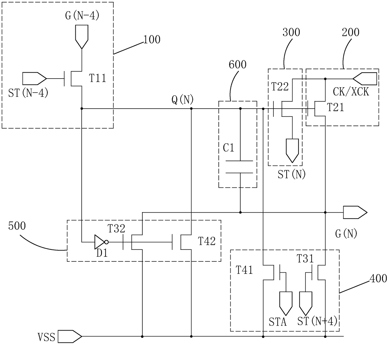
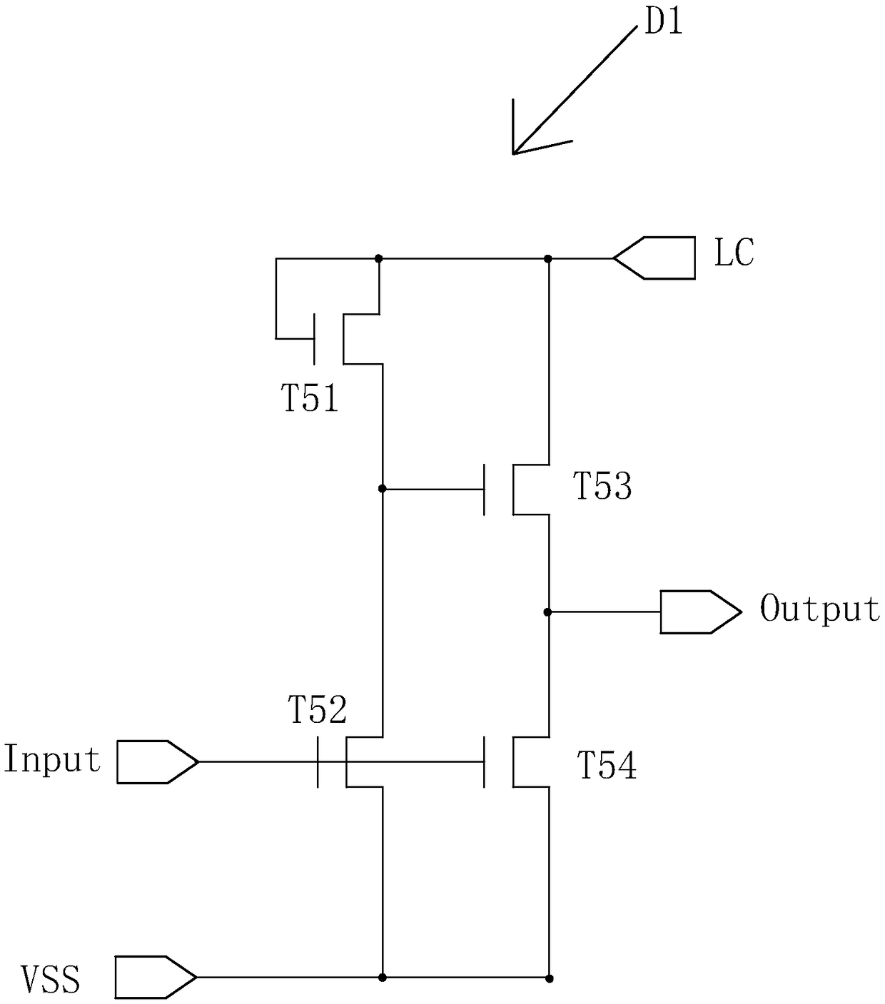
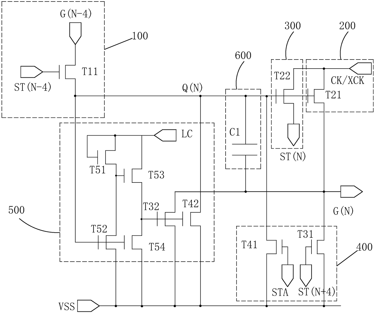
[0037] see figure 1 , the present invention provides a GOA circuit, including a plurality of cascaded GOA units, each level of GOA unit includes a pull-up control module 100, a pull-up module 200, a downlink module 300, a pull-down module 400, a pull-down maintenance module 500 and bootstrap module 600;

[0038] Let N be a positive integer, except for the GOA units of the first to fourth levels and the GOA units of the penultimate level to the last level, in the Nth level of GOA units,

[0039]The pull-up control module 100 is connected to the stage transmission signal ST(N-4) of the N-4th level GOA unit and the scanning signal G(N-4) of the N-4th level GOA circuit, for The level transmission signal ST(N-4) of the 4th level GOA unit and the ...


PUM


Abstract

The invention provides a GOA circuit. According to the GOA circuit, the level transmission signal and the pull-down level transmission signal of the N+4th GOA unit are arranged in the pull-down moduleof the Nth GOA unit to replace the scanning signal of an N+4th GOA unit in the traditional GOA circuit, so that a pull-up module can pull up the electric potential of the scanning signal, and also can pull down the electric potential of the scanning signal, and the electric potential of the scanning signal can be effectively pulled down to a direct-current low potential in a short time, the problems of level transmission failure and pixel mischarging of the GOA circuit are avoided, and the load of the scanning signal can also be reduced, the output waveform of the scanning signal is optimized, and the charging condition of the pixel in the liquid crystal panel is improved.

Description

technical field [0001] The invention relates to the field of display technology, in particular to a GOA circuit. Background technique [0002] Thin Film Transistor (TFT) is the main driving element in current Liquid Crystal Display (LCD) and Active Matrix Organic Light-Emitting Diode (AMOLED). It is related to the display performance of the flat panel display device. [0003] Most of the liquid crystal displays currently on the market are backlight liquid crystal displays, which include a liquid crystal display panel and a backlight module. The working principle of the liquid crystal display panel is to pour liquid crystal molecules between the thin film transistor substrate (Thin FilmTransistor Array Substrate, TFT Array Substrate) and the color filter (Color Filter, CF) substrate, and apply pixel voltage on the two substrates respectively. and the common voltage, through the electric field formed between the pixel voltage and the common voltage to control the rotation di...

Claims


Application Information

Patent Timeline
Patent Type & Authority Applications(China)
IPC IPC(8): G09G3/36
CPCG09G3/3677
Inventor 陈帅
Owner TCL CHINA STAR OPTOELECTRONICS TECH CO LTD
Learn More