
Light emitting device and manufacturing method thereof
A manufacturing method and technology for light-emitting devices, which are applied to semiconductor devices, electrical components, circuits, etc., can solve the problems of increasing the number of manufacturing processes, declining performance of light-emitting devices, and low product competitiveness, reducing the number of process processes and eliminating solvents. The effect of poor vapor concentration and shortening of the printing process
- Summary
- Abstract
- Description
- Claims
- Application Information
AI Technical Summary
Problems solved by technology
Method used
Image

Examples
Embodiment 1
[0113] This embodiment provides a method for manufacturing a printed display, which includes the following steps:
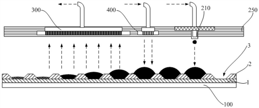
[0114] 1) Prepare a pixel defining layer 2 on a patterned anode TFT substrate 1, and form a pixel pit 3.
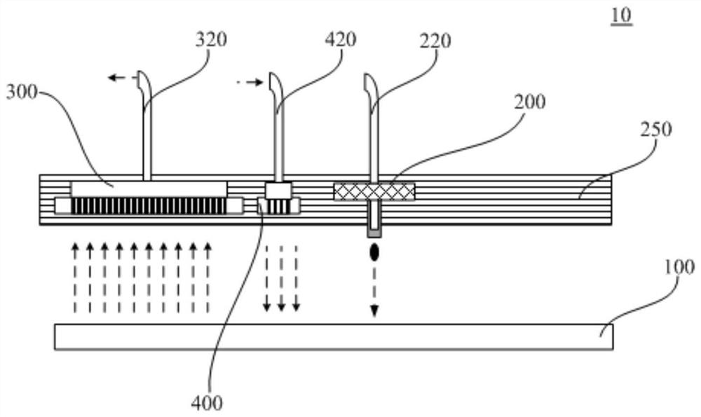
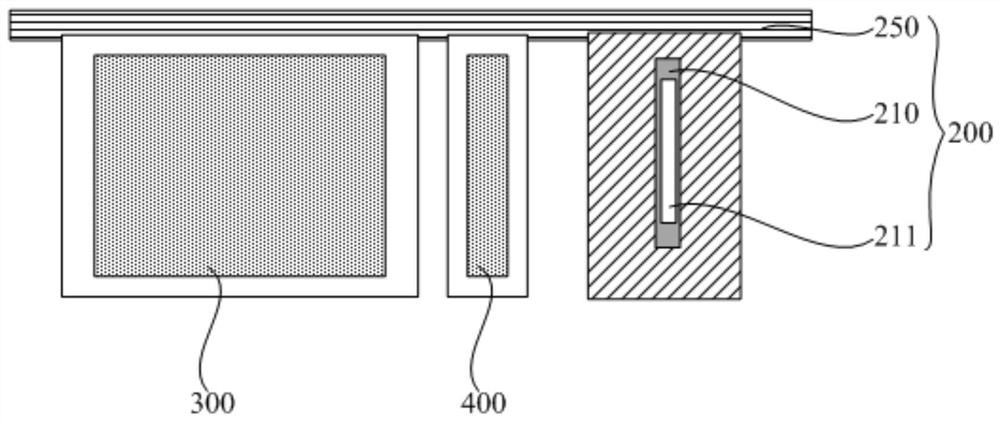
[0115] 2), please further combine image 3 , using the printing device 10 to ink-jet print functional ink into the pixel pit 3, and perform step-by-step vacuum drying treatment on the printed ink to obtain a pre-dried film.
[0116] 3) heat-treating the pre-dried film to make it completely cross-linked and cured to form a light-emitting functional layer.
[0117] Wherein, the light-emitting functional layer includes a hole injection layer, a hole transport layer, and a light-emitting layer, and the formation process of each layer adopts a step-by-step vacuum drying process while inkjet printing is performed.
[0118] 4), evaporating the electron transport layer and the cathode, and finally packaging, that is.
[0119] This embodiment provides a method for...
PUM
 Abstract
Description
Claims
Application Information