

A defect detection method for plastic package IC chips based on feature template matching and deep learning
A technology of deep learning and feature templates, which is applied in the direction of optical testing flaws/defects, measuring devices, scientific instruments, etc., and can solve problems such as defect identification, low accuracy of defect classification, and unclear printing information of pin chips
- Summary
- Abstract
- Description
- Claims
- Application Information
AI Technical Summary
Problems solved by technology
Method used
Image

Examples
Embodiment Construction
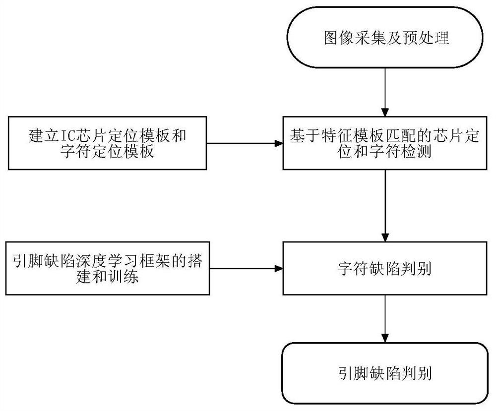
[0051] like figure 1 As shown, a method for defect detection of plastic encapsulated IC chips based on feature template matching and deep learning includes the following steps:
[0052] (1) Image acquisition and preprocessing
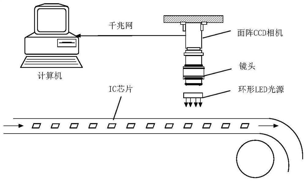
[0053] The IC chip image in the high-speed feeder is collected by a high frame rate CCD camera, and the image is preprocessed. First of all, in order to improve the quality of image acquisition, the red LED light source is fixed directly below the camera, such as figure 2 shown. Then, image filtering is performed on the collected target image to remove the noise signal existing in the image. Finally, a grayscale enhancement algorithm is used to improve the contrast of the image.
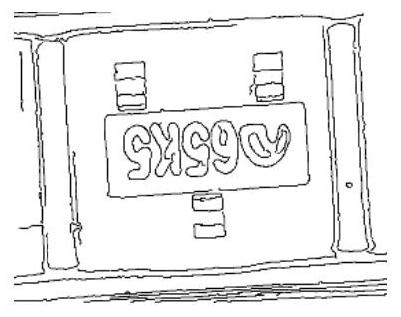
[0054] (2) Establish IC chip positioning template and character positioning template
[0055] The establishment of the IC chip positioning template and the character positioning template of the present invention is to use the edge detection method to locate the edge poin...
PUM
 Abstract
Description
Claims
Application Information