

Substrate, display panel, display device, and preparation method of display panel
A technology for display panels and substrates, which is used in final product manufacturing, sustainable manufacturing/processing, semiconductor/solid-state device manufacturing, etc. to achieve consistent resolution and multi-angle viewing.
- Summary
- Abstract
- Description
- Claims
- Application Information
AI Technical Summary
Problems solved by technology
Method used
Image

Examples
Embodiment Construction
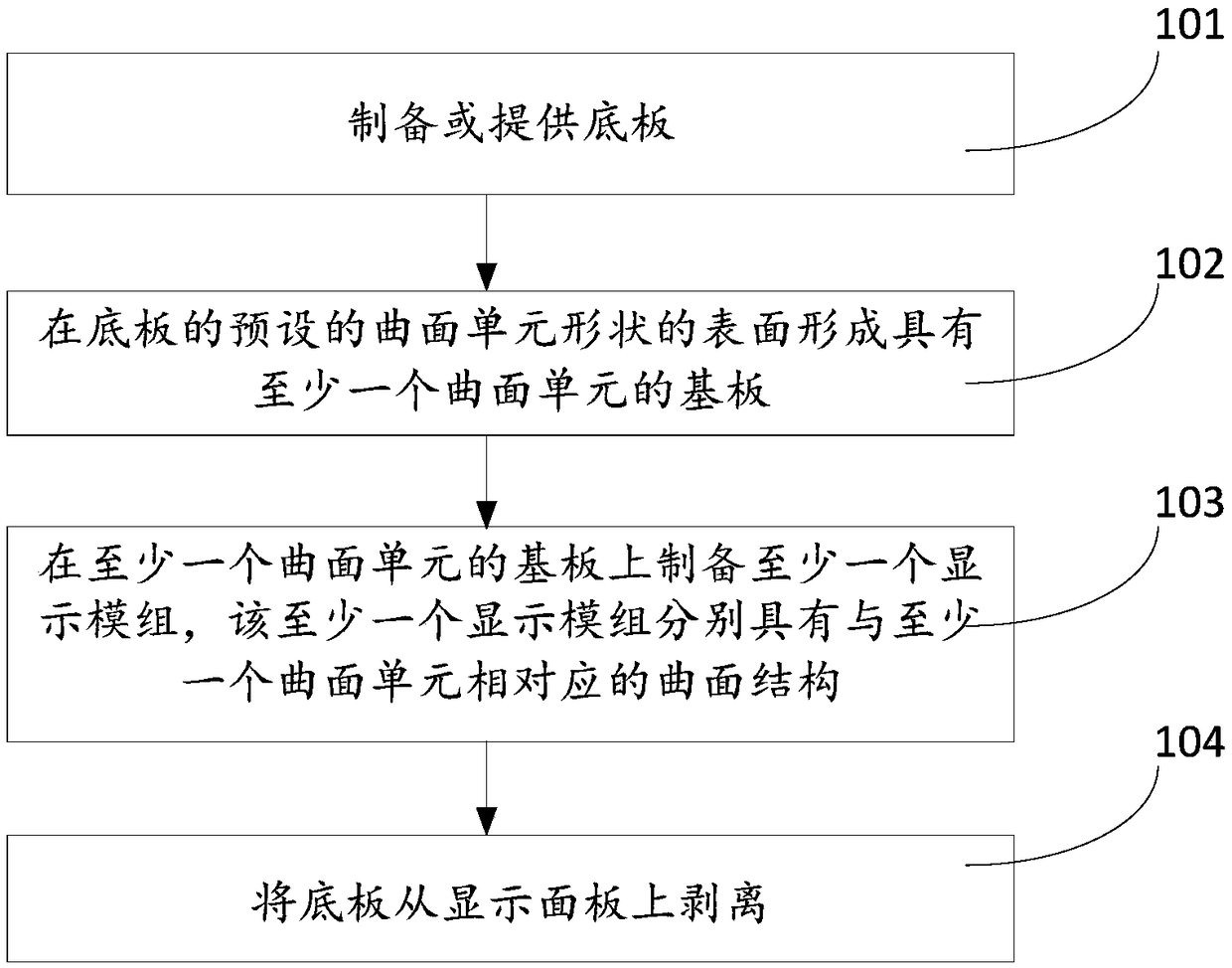
[0041] The following will clearly and completely describe the technical solutions in the embodiments of the present invention with reference to the accompanying drawings in the embodiments of the present invention. Obviously, the described embodiments are only some of the embodiments of the present invention, not all of them. Based on the embodiments of the present invention, all other embodiments obtained by persons of ordinary skill in the art without creative efforts fall within the protection scope of the present invention.
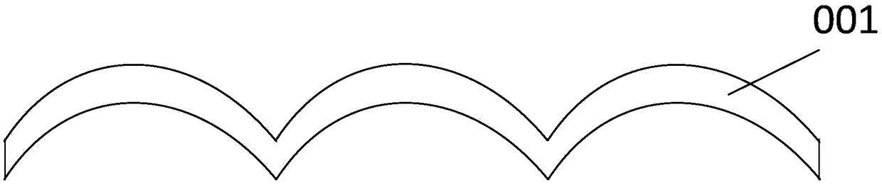
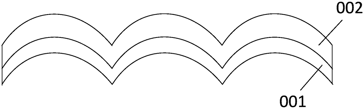
[0042] figure 1 Shown is a schematic structural view of the bottom plate provided by an embodiment of the present invention.
[0043] like figure 1 As shown, the substrate 001 includes at least one curved surface unit. Since the shape of the substrate 001 includes at least one curved surface shape, the shape of the display panel prepared on the surface of the substrate 001 should correspond to the shape of the substrate 001. The shape of the display ...
PUM
 Abstract
Description
Claims
Application Information