Shell of an electronic device, a manufacturing method thereof and an electronic device

A technology for electronic equipment and housing, which is applied to the housing of electronic equipment and its manufacture, and the fields of electronic equipment, can solve the problems of unrealizable, single apparent color of the anodized layer, and changing appearance effects, so as to meet the needs of appearance effects. , The effect of increasing market competitiveness and fashionable appearance

Inactive Publication Date: 2018-12-21
GUANGDONG OPPO MOBILE TELECOMM CORP LTD
View PDF5 Cites 8 Cited by
  • Summary
  • Abstract
  • Description
  • Claims
  • Application Information

AI Technical Summary

Problems solved by technology

[0002] At this stage, due to the serious homogeneity and aesthetic fatigue of the casings of electronic devices such as mobile phones, tablet computers, and smart watches, the surface effect of a single color can no longer meet consumers' needs for changing appearance effects of electronic devices.
Moreover, the commonly used material for the housing of electronic equipment is aluminum alloy, and its surface needs to be anodized. However, the apparent color of the anodized layer is single, and it is impossible to achieve changing appearance effects.

Method used


Image

  • Shell of an electronic device, a manufacturing method thereof and an electronic device
  • Shell of an electronic device, a manufacturing method thereof and an electronic device
  • Shell of an electronic device, a manufacturing method thereof and an electronic device

Examples


Embodiment Construction

[0027] The following describes the embodiments of the present invention in detail, and those skilled in the art will understand that the following embodiments are intended to explain the present invention, and should not be regarded as limiting the present invention. Unless otherwise specified, in the following examples that do not explicitly describe specific techniques or conditions, those skilled in the art can carry out according to commonly used techniques or conditions in this field or according to product instructions.

[0028] In one aspect of the embodiments of the present invention, a casing of an electronic device is provided.

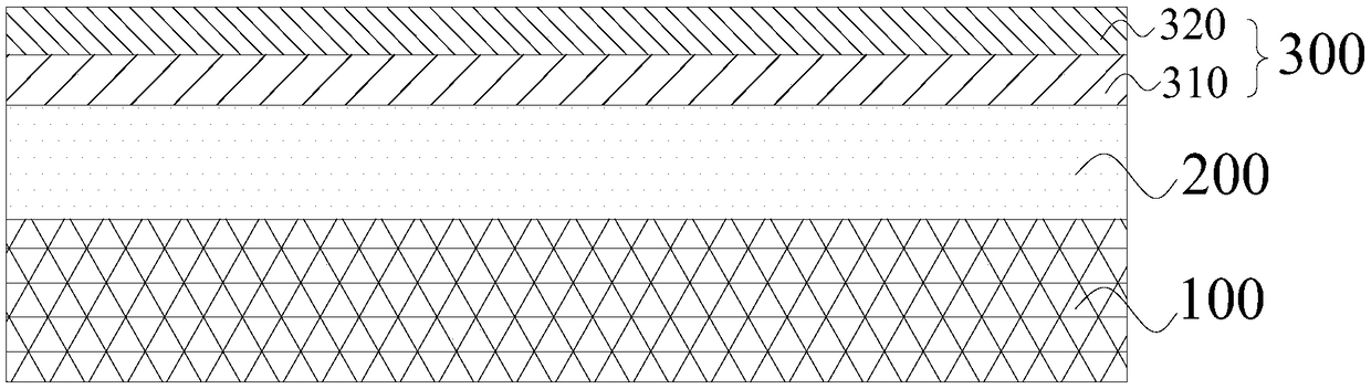
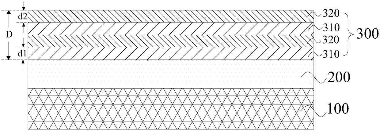
[0029] According to an embodiment of the present invention, refer to figure 1 , the casing of the electronic device includes a casing body 100, an anodized layer 200, and an optical film layer 300 stacked in layers, wherein the optical film layer 300 includes a plurality of first sub-film layers 310 and a plurality of second sub-film layers ...


PUM

PropertyMeasurementUnit
thicknessaaaaaaaaaa
thicknessaaaaaaaaaa
thicknessaaaaaaaaaa

Abstract

The invention provides a shell of an electronic device, a manufacturing method thereof and an electronic device. The shell of the electronic device includes a shell body, an anodic oxide layer and anoptical film layer, wherein the optical film layer includes a plurality of first sub-film layers and a plurality of second sub-film layers arranged alternately, and the first sub-film layer is formedof silicon oxide, and the second sub-film layer is formed of at least one of titanium oxide and niobium oxide. In the shell ofthe electronic device according to the present invention, an optical filmlayer is also arranged on the anodic oxide layer on the surface of the shell body, and the optical film layer is a plurality of layer of silicon oxide and titanium oxide or silicon oxide and niobium oxide alternately arranged, thus, the light is refracted many times between the film layers with different refractive indices, thereby realizing a magic color discoloration effect such as a rainbow onthe surface of the shell, and further enabling the appearance of the electronic device to meet the needs of consumers for the changeable appearance effect of the electronic device.

Description

technical field [0001] The present invention relates to the technical field of shell production of electronic equipment, and in particular, the present invention relates to a shell of electronic equipment, a manufacturing method thereof, and electronic equipment. Background technique [0002] At this stage, due to serious homogenization and aesthetic fatigue of the casings of electronic devices such as mobile phones, tablet computers, and smart watches, the surface effect of a single color can no longer meet consumers' needs for changing appearance effects of electronic devices. Moreover, aluminum alloy is commonly used as the housing of electronic equipment, and its surface needs to be anodized. However, the apparent color of the anodized layer is single, and it is impossible to achieve changing appearance effects. Contents of the invention [0003] An object of the embodiments of the present invention is to provide a casing structure of an electronic device, a method for...

Claims


Application Information

Patent Timeline
Patent Type & Authority Applications(China)
IPC IPC(8): H04M1/02B44C5/04B44C3/02
CPCB44C3/02B44C5/0446H04M1/0283
Inventor 陈颖杨光明
Owner GUANGDONG OPPO MOBILE TELECOMM CORP LTD
Why Eureka
Try Eureka