
A Wide Bandwidth Angular Scanning Phased Array Antenna Based on Triangular Grid Arrangement
A phased array antenna, wide-angle scanning technology, applied in antennas, resonant antennas, antenna arrays and other directions, can solve the problem of not involving bandwidth, no unit model is given, etc., to reduce the number of array elements, reduce the profile, Easy-to-process effects
- Summary
- Abstract
- Description
- Claims
- Application Information
AI Technical Summary
Problems solved by technology
Method used
Image

Examples
Embodiment 1
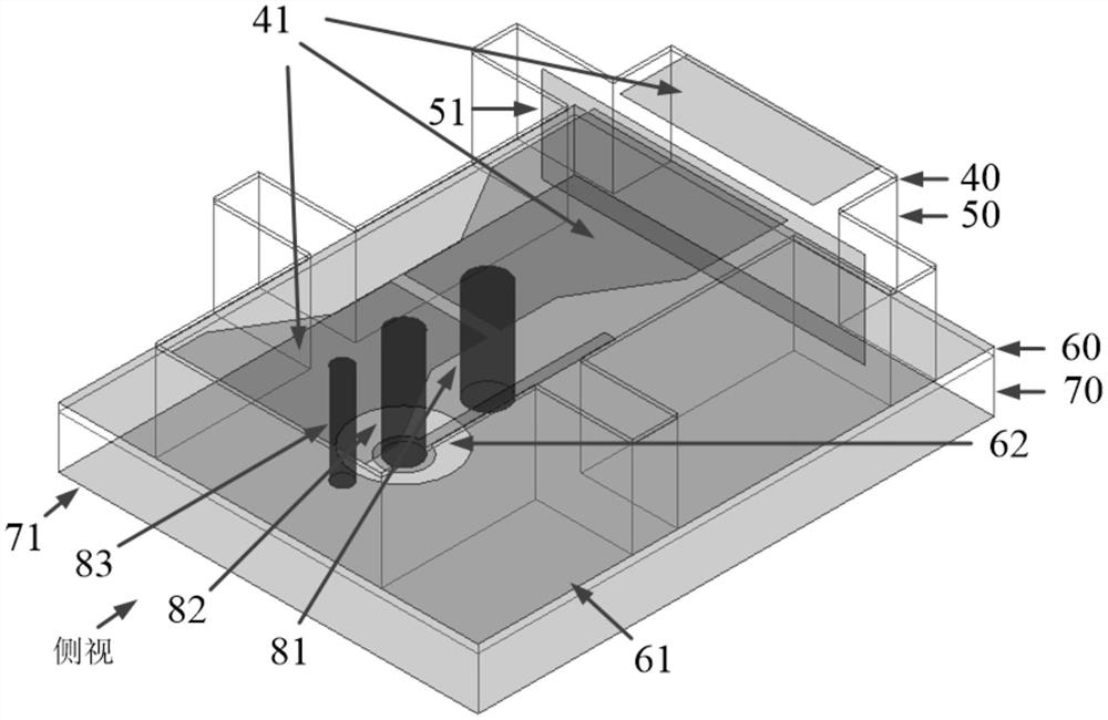
[0021] The antenna of this embodiment works at 7-13 GHz, and its unit structure 3D view, side view, and top view are shown in Figures 1-3 respectively, and the size of the array element is 16mm×13mm, which is about 0.69λ h ×0.56λ h (λ h for the wavelength of 13GHz).
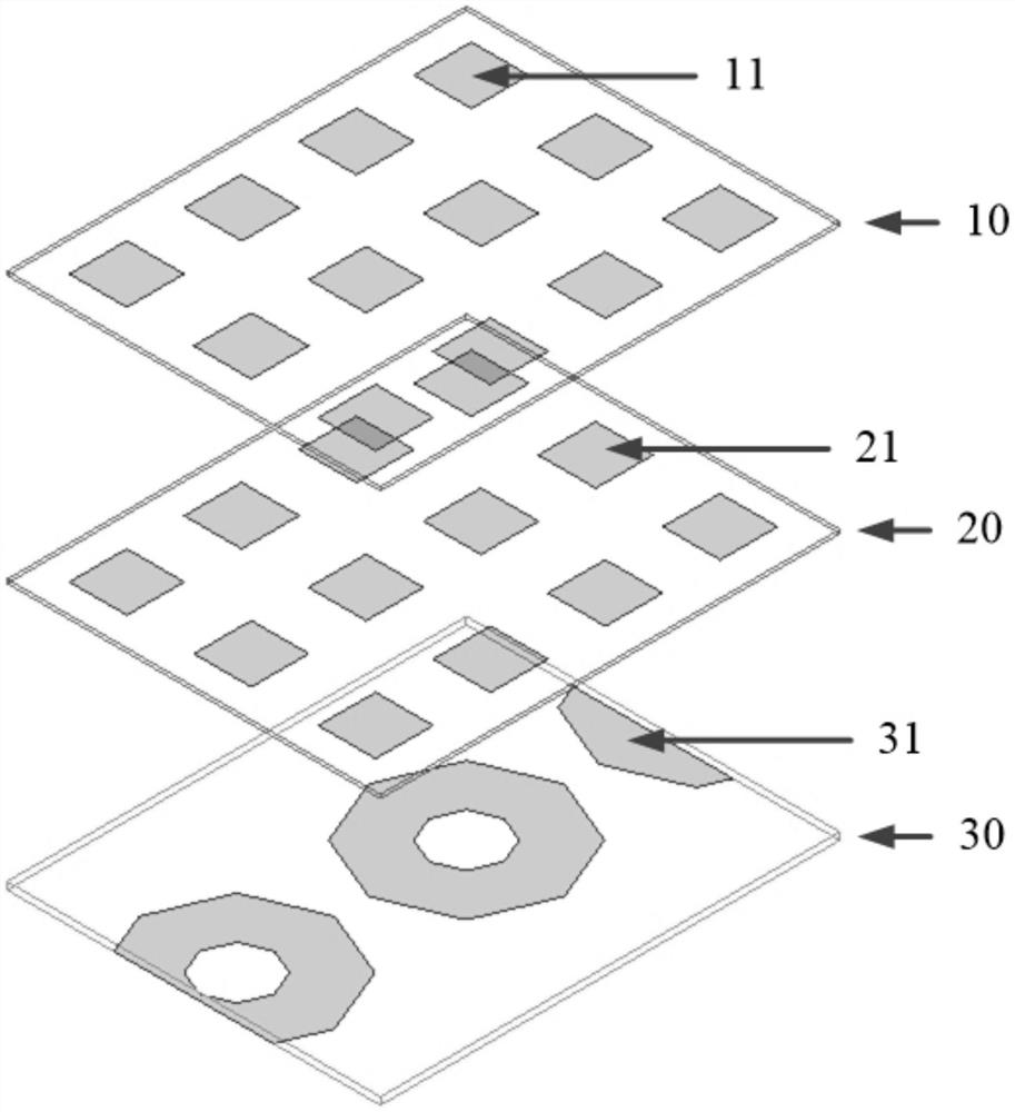
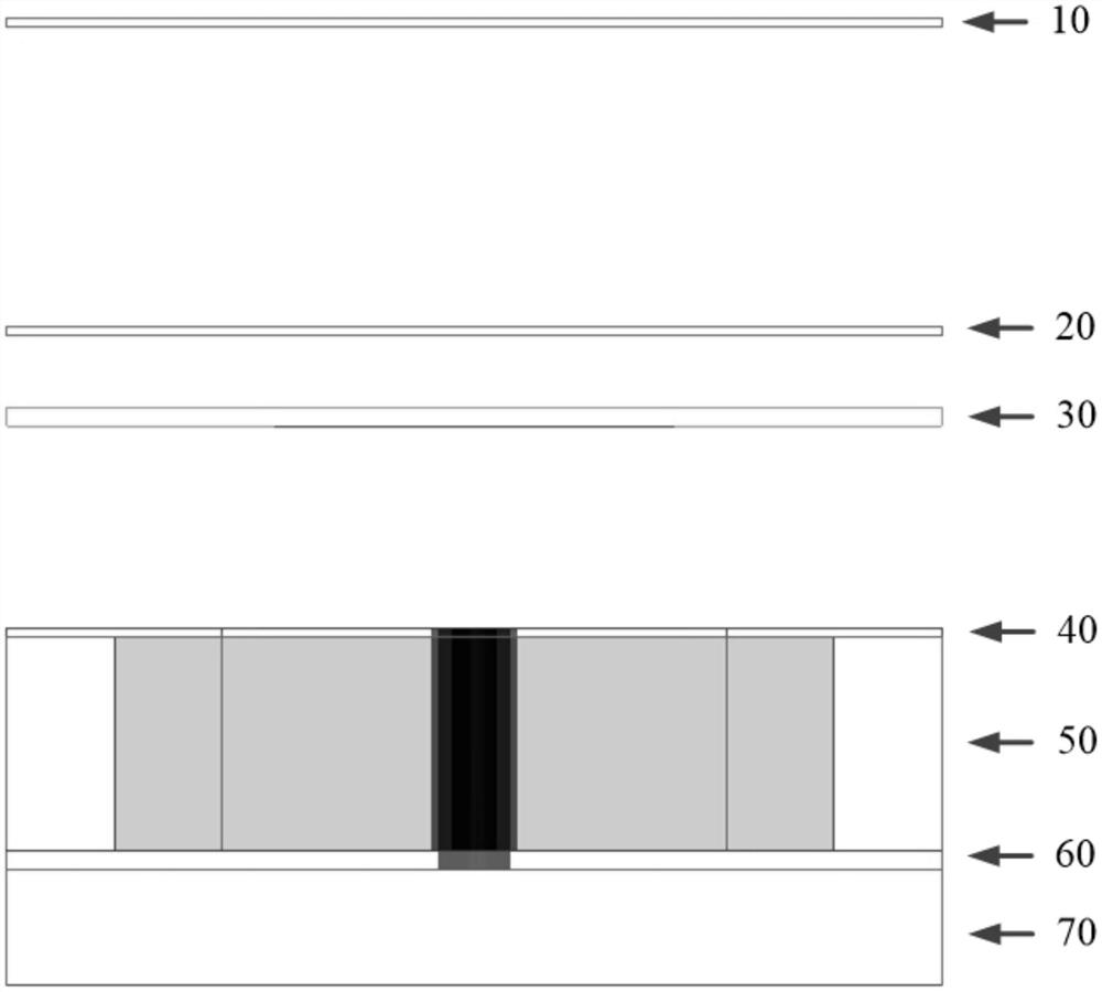
[0022] The antenna consists of two layers of metamaterial wide-angle matching layers 10 and 20 from top to bottom, and a layer of non-marginal parasitic patch layer 30, as shown in Figure 1(a). The antenna layer is a dielectric laminated structure, including 40 to 70 layers, see Figure 1(b), the vertical distribution of each layer is shown in figure 2 .
[0023] The thicknesses of the first to fourth dielectric substrates 40 to 70 of the antenna layer are 0.127 mm, 2.973 mm, 0.254 mm, and 1.624 mm in sequence, and the relative dielectric constants are all 2.94.
[0024] The dipole unit 41 is printed on the upper surface of the first dielectric substrate 40, see image 3 (a); the first metal floor 61 is betwe...
PUM
 Abstract
Description
Claims
Application Information