Silk-screen anti-adhesion PCB nail bed template

An anti-adhesion, screen printing technology, applied in screen printing machines, printing, printing machines, etc., can solve the problems of low efficiency, waste of time, long waiting time, etc., and achieve the effect of improving efficiency

Inactive Publication Date: 2019-03-01
鹤山市泰利诺电子有限公司
View PDF0 Cites 0 Cited by
  • Summary
  • Abstract
  • Description
  • Claims
  • Application Information

AI Technical Summary

Problems solved by technology

[0004] In the process of PCB board processing, the PCB circuit board needs to be screen-printed. In the traditional screen-printing process, usually someone manually puts the screen-printing mold on the circuit board. Long time, waste of time, inefficiency

Method used


Image

  • Silk-screen anti-adhesion PCB nail bed template
  • Silk-screen anti-adhesion PCB nail bed template

Examples


Embodiment Construction

[0016] Embodiments of the present invention are described in detail below, examples of which are shown in the drawings, wherein the same or similar reference numerals designate the same or similar elements or elements having the same or similar functions throughout. The embodiments described below by referring to the figures are exemplary and are intended to explain the present invention and should not be construed as limiting the present invention.

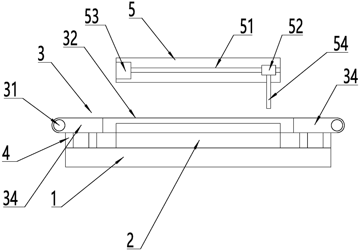
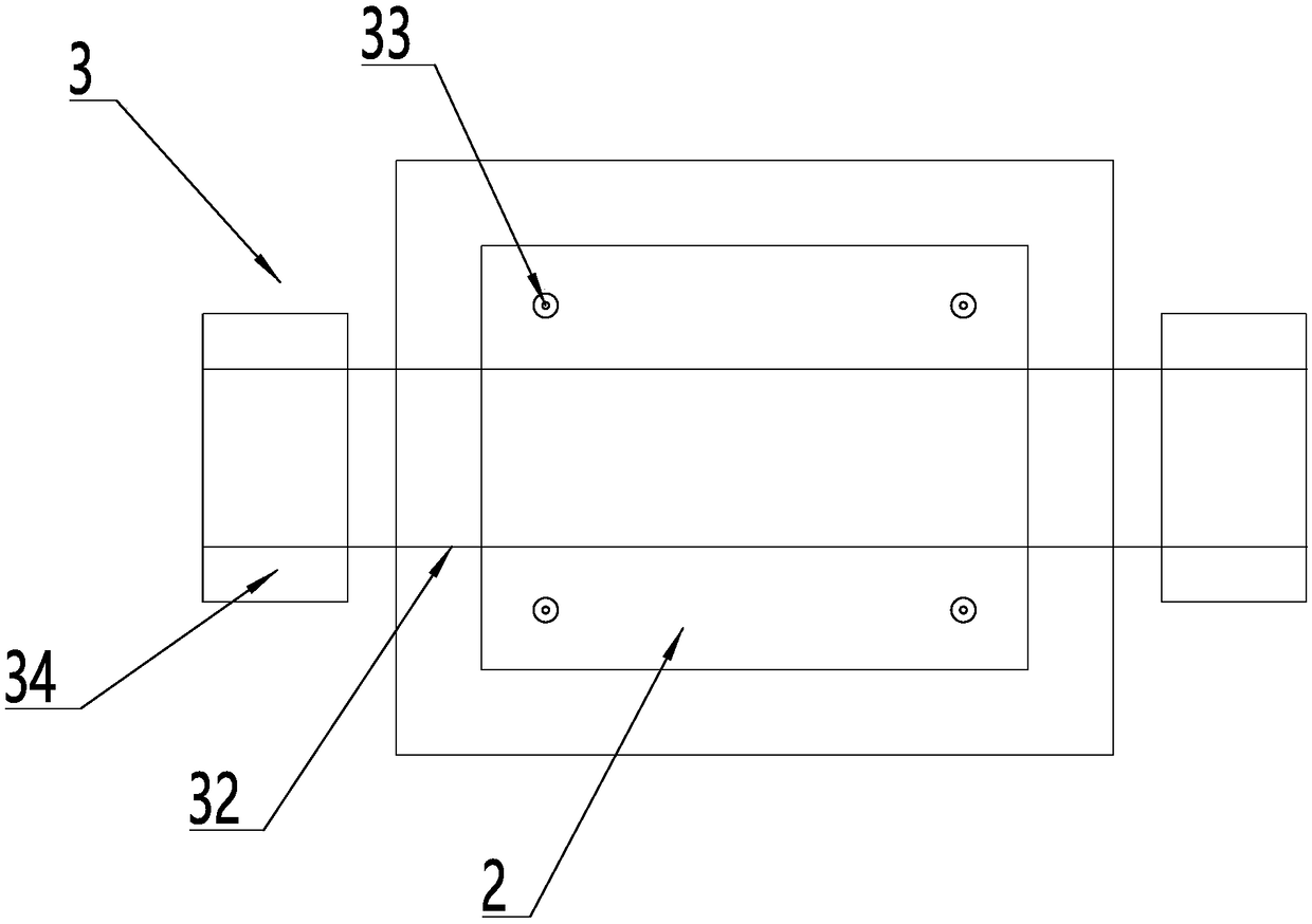
[0017] refer to figure 1 and figure 2 , an anti-adhesion PCB nail bed template for silk screen printing, including a base 1, a screen printing platform 2 is installed on the base 1, and a conveying device 3 for loading workpieces arranged on both sides of the silk printing platform 2, the conveying device 3 includes a lifting mechanism 4, and the conveyor belt 32 mechanism installed on the lifting mechanism 4. The conveyor belt 32 mechanism includes transmission wheels 31 respectively arranged on both sides of the screen printi...


PUM


Abstract

The invention discloses a silk-screen anti-adhesion PCB nail bed template which comprises a base. A silk-screen platform and conveying devices arranged on the two sides of the silk-screen platform andused for workpiece feeding are mounted on the base. The conveying devices comprise a lifting mechanism and a conveying belt mechanism mounted on the lifting mechanism. The conveying belt mechanism comprises drive wheels arranged on the two sides of the silk-screen platform correspondingly and a conveying belt annularly arranged on the two drive wheels in a sleeving manner. An empty groove used for allowing the conveying belt to pass is formed in the silk-screen platform, and protrusions used for bearing workpieces are evenly distributed on the silk-screen platform. The workpieces are transported to the silk-screen platform through the conveying device capable of ascending and descending and are located on the protrusions, gaps are kept between the workpieces and the silk-screen platform by means of bearing of the protrusions, the workpieces can be turned over to achieve silk-screen printing of the other faces after silk-screen printing of one faces of the workpieces is completed, andthe silk-screen printing is improved.

Description

technical field [0001] The invention relates to the field of PCB manufacturing, in particular to an anti-adhesion PCB nail bed template for silk screen printing. Background technique [0002] Printed circuit board (PCB board), also known as printed circuit board, uses an insulating board as the base material and cuts it to a certain size. At least one conductive pattern is attached to it as the substrate, and holes (such as component holes) are provided on the upper part of the substrate. , strong holes, metal holes and other mounting holes), used to replace the chassis of electronic components installed in the past, and realize the electrical connection between component pins through conductive patterns, pads and metallized vias on the substrate. As the most basic and core component of electronic products, printed circuit boards are widely used in various electronic products and large equipment and devices. [0003] At present, the output value of the global printed circui...

Claims


Application Information

Patent Timeline
Patent Type & Authority Applications(China)
IPC IPC(8): B41F15/18
CPCB41F15/18
Inventor 詹贵全
Owner 鹤山市泰利诺电子有限公司
Why Eureka
Try Eureka