Check patentability & draft patents in minutes with Patsnap Eureka AI!

Semiconductor wafer cleaning equipment

A technology for cleaning equipment and semiconductors, which is applied in semiconductor/solid-state device manufacturing, cleaning methods using liquids, cleaning methods, and utensils, and can solve problems that are not fully satisfied

Active Publication Date: 2021-08-27
TAIWAN SEMICON MFG CO LTD
View PDF5 Cites 1 Cited by
  • Summary
  • Abstract
  • Description
  • Claims
  • Application Information

AI Technical Summary

Problems solved by technology

[0004] Although existing manufacturing machines are generally sufficient to meet their needs, they are still not fully satisfied

Method used


Image

  • Semiconductor wafer cleaning equipment
  • Semiconductor wafer cleaning equipment
  • Semiconductor wafer cleaning equipment

Examples


Embodiment Construction

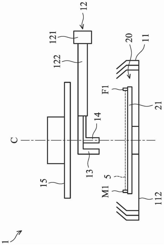
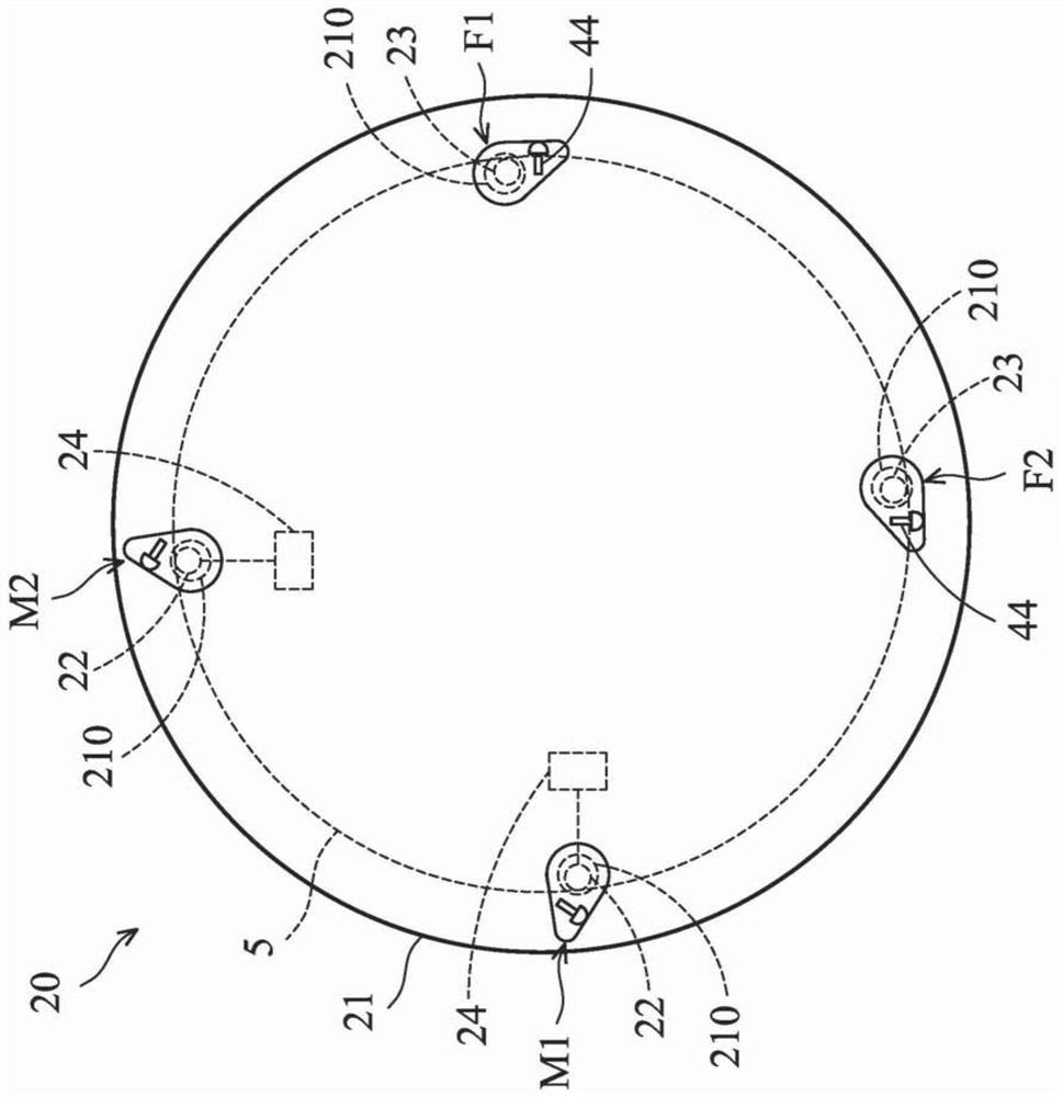
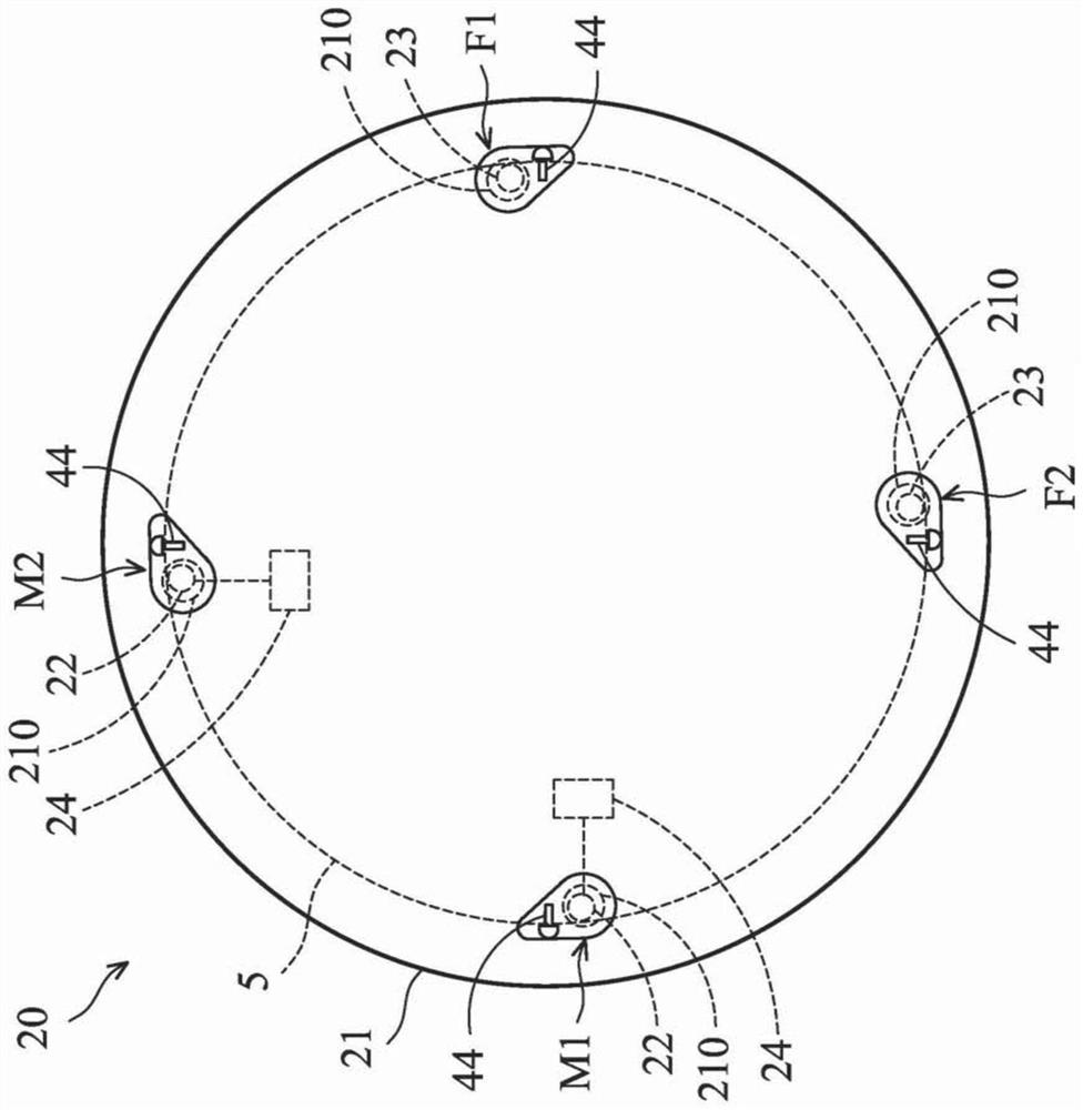
[0078]The following disclosure provides many different embodiments or examples for implementing different features of the present invention. The following disclosure describes specific examples of various components and their arrangements to simplify the description. Of course, these specific examples are not intended to be limiting. For example, if an embodiment of the present invention discloses that a first feature is formed on or above a second feature, it means that it may include an embodiment in which the above-mentioned first feature is in direct contact with the above-mentioned second feature, and may also include Embodiments in which an additional feature is formed between the first feature and the second feature such that the first feature and the second feature may not be in direct contact. In addition, the same reference signs and / or symbols may be reused in different examples in the following publications. These repetitions are for simplicity and clarity and ar...


PUM


Abstract

An embodiment of the present disclosure provides semiconductor wafer cleaning equipment. The semiconductor wafer cleaning equipment includes a rotating base with a through hole. The semiconductor wafer cleaning apparatus further includes a shaft extending through the through hole. The semiconductor wafer cleaning equipment also includes a clamping piece. The clamping piece covers the through hole and is connected to the rotating shaft. The rotating shaft communicates with a gap in the through hole. The gap is formed between the rotating base and the clamping piece. In addition, the semiconductor wafer cleaning device includes a sealing ring adjacent to the gap and located farther from the rotating shaft than the gap.

Description

technical field [0001] The embodiment of the present invention relates to a semiconductor wafer cleaning device, in particular to a semiconductor wafer cleaning device with a clamping mechanism and a sealing structure. Background technique [0002] The semiconductor integrated circuit (IC) industry has grown exponentially, and technological advancements in integrated circuit materials and design have produced multiple eras of integrated circuits, and each era has smaller and more complex circuits than the previous era. During the development of integrated circuits, functional density (ie, the number of interconnects per chip area) typically increases as geometry size (ie, the smallest component or circuit that can be produced in a process) shrinks. . This downscaling process increases production efficiency and reduces associated costs. This shrinking process also increases the complexity of manufacturing and producing integrated circuits. [0003] One or more wafers are u...

Claims


Application Information

Patent Timeline
Patent Type & Authority Patents(China)
IPC IPC(8): H01L21/67
CPCH01L21/67017H01L21/67051H01L21/68728H01L21/02057H01L21/6704H01L21/304B08B1/001H01L21/0206B08B1/04B08B3/024B08B1/007
Inventor 陈嘉伦施博仁洪明松许文鸿
Owner TAIWAN SEMICON MFG CO LTD
Features
  • R&D
  • Intellectual Property
  • Life Sciences
  • Materials
  • Tech Scout
  • Unparalleled Data Quality
  • Higher Quality Content
  • 60% Fewer Hallucinations
Learn More