Security marking and security mark

a technology of security marks and markings, applied in the field of security markings, can solve the problems of increasing cost and complexity,

Inactive Publication Date: 2005-07-21
DOUGLAS JOEL S
View PDF51 Cites 182 Cited by
  • Summary
  • Abstract
  • Description
  • Claims
  • Application Information

AI Technical Summary

Benefits of technology

[0033] It is an advantage of the present invention to provide an improved security marking system which can be used as an individual identification system, gaming mark or a security mark for identification of forged or non licensed product replicas.
[0034] In preferred embodiments, the present invention provides security marking comprising at least one layer of conductive material which withstands any attempt to forge the information encoded thereon and thus resists any attempted forgery of the information fixed in the conductive layer of the security marking.
[0035] In accordance with the present invention, an algorithm which registers a fingerprint by indicating the quality of a fingerprint image by pseudo minutia can be used with the present invention to capture the fingerprint information in the conductive material and using this image as an identification system.
[0036] In accordance with the present invention, the layer of conductive material can comprise numerous materials, including, but not limited to, conductive inks, plastics and coatings.
[0037] The present invention provides, a security marking having a single layer of conductive material containing at least one element of conductively readable identifying indicia. This conductive layer can be made by applying a conductive film to the surface of a security card or to a product “tag”. The conductive layer is formed from a film that has a surface resistance in the range of less than about 150,000 ohms / square, or more preferably about 25,000 ohms / square.
[0038] In preferred aspects, the layer of conductive material can be formed from a variety of conductive films, coatings or inks, including, but not limited to those described in U.S. patent application 2002 / 0143094 entitled Polymer Nanocomposites and Methods of Preparation, Conroy, Jeffrey L., et. al.; U.S. patent application 2002 / 0035170 entitled Electromagnetic Shielding Composite Comprising Nano Tubes, Glatkowski, Paul; et al; U.S. patent application 2002 / 0180077 entitled Carbon Nano Tube Fiber-Reinforced Composite Structures for EM and Lightning Strike Protection, Glatkowski, Paul; et al; U.S. patent application 2003 / 0008123 entitled Nanocomposite Dielectrics, Glatkowski, Paul; et al; U.S. patent application 2003 / 0164427 entitled ESD Coatings For Use With Spacecraft, Glatkowski, Paul; et al; and U.S. patent application 2003 / 0122111 entitled Coatings Comprising Carbon Nano Tubes and Methods For Forming Same, Glatkowski, Paul; et al; all included herein by reference. The dispersion that form the conductive material can be further comprising a plasticizer, softening agent, filler, reinforcing agent, processing aid, stabilizer, antioxidant, dispersing agent, binder, a cross-linking agent, a coloring agent, a UV absorbent agent, or a charge adjusting agent.

Problems solved by technology

When it is laminated to paper cores, it is unfortunately a disadvantage that these laminations can be opened up relatively easily and are thus accessible to manipulations and forgeries of any kind.
However the need to have the data stored on a processing unit increases the cost and complexity.
However, since the two dimensional code can be read by conventional means the two dimensional code can be readily forged because it does not have a built in verifying mechanism to allow the reader to check for authenticity.

Method used


Image

  • Security marking and security mark
  • Security marking and security mark
  • Security marking and security mark

Examples


Embodiment Construction

(a) General Description:

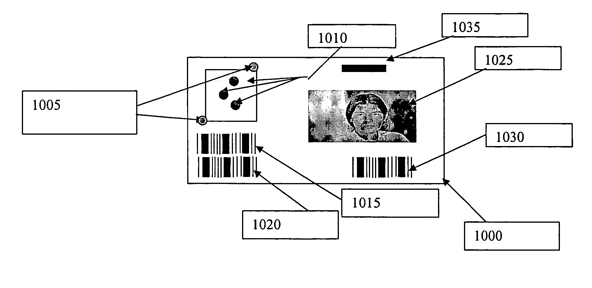
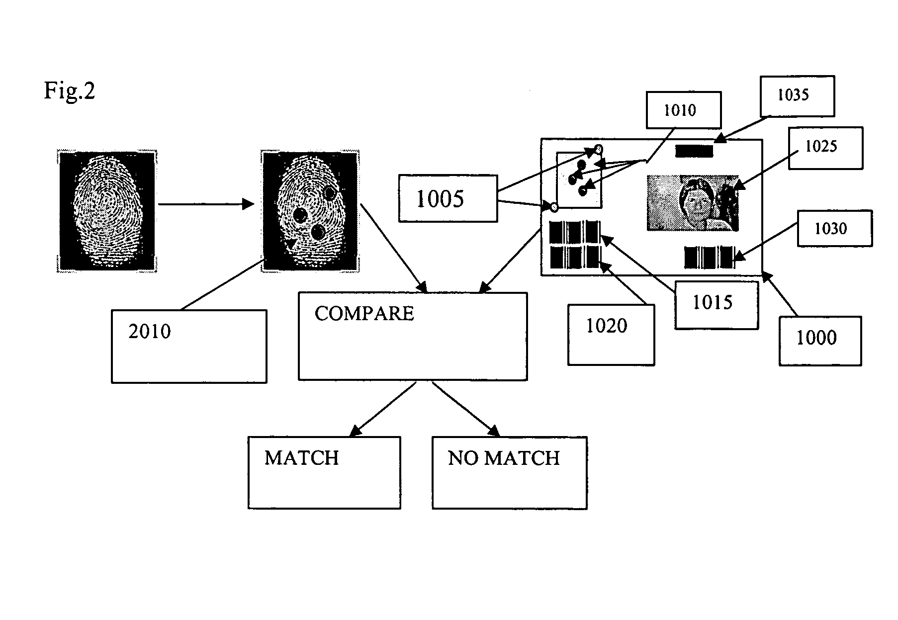
[0065] The present invention provides a security marking or identity “tag” that can be affixed to a security card, or to a product label, or to a product itself. In one embodiment of the invention, the identity tag is composed of at least two layers wherein one layer carries identification information such as the name, photograph and personal reference number, and the other layer carries additional latent security markings represented by a layer comprising a pattern of conductive materials either inscribed in or printed thereon. The two individual layers of the security marking may have different transparencies. For example, the first of the two layers may comprise the core (i.e.: main body) of a security card, and have a matt, preferably white, coloring as a result of added pigment with moderate to low transparency. By contrast, the conductive layer of the security marking may have a very high transparency. Therefore, the conductive layer may be applied di...


PUM


Abstract

The application discloses a security mark consisting of a plurality of layers, of which the cover layers are highly conductive films and the layers of the card core are films of varying transparency. One layer carries information, which can be read directly, if desired, above a security print, while the transparent conductive layer has an additional security markings, such as biometric or product identifiers marking which can be read conductively only with the aid of a special reader. All the layers consist of polymers, papers or mixtures which can be fused together to form a laminate which is fused together. The conductive layers form conductive traces which may be formed with single-walled or multi walled nano tubes or they can be formed from multiple layers or dispersions containing, carbon nano tubes, carbon nano tubes / antimony tin oxide, carbon nano tubes / platinum, or carbon nano tubes / silver, carbon, silver or carbon nano tubes / silver-cloride. An alternative layer can be formed from a separate conductive layer or suitable dispersion and the encoding accomplished by overlaying a nonconductive trace.

Description

REFERENCE TO RELATED APPLICATIONS [0001] This invention claims priority to U.S. Provisional Application No. 60 / 536,775 entitled Identity Card, filed on Jan. 15, 2004.FIELD OF THE INVENTION [0002] The present invention relates to a security marking formed from a layer of conductive materials that is patterned so as to have identification information captured therein. The conductive coating layer may be formed by printing, etching, or formulation. The conductive layer can be made from carbon nano tube conductive ink, conductive films or conductive inks formed from metals and oxides, but is not so limited. As will be shown, the conductive coating layer may be applied to security cards, or directly to products to prevent counterfeiting. [0003] In preferred embodiments, the present invention relates to a security marking consisting of several layers of materials. For example, the present security marking may consist of a layer of conductive material sections with an overlying layer of pr...

Claims


Application Information

Patent Timeline
Patent Type & Authority Applications(United States)
IPC IPC(8): G06K19/18H01L23/52
CPCG06K19/18B82Y10/00
Inventor DOUGLAS, JOEL S.
Owner DOUGLAS JOEL S
Why Eureka
Try Eureka