Method for forming a via contacting several levels of semiconductor layers
a technology of semiconductor layers and vias, applied in the field of integrated circuits, can solve the problems of increasing the stray capacitance between the gate and the source and drain regions of the upper level transistors
- Summary
- Abstract
- Description
- Claims
- Application Information
AI Technical Summary
Benefits of technology
Problems solved by technology
Method used
Image
Examples
Embodiment Construction
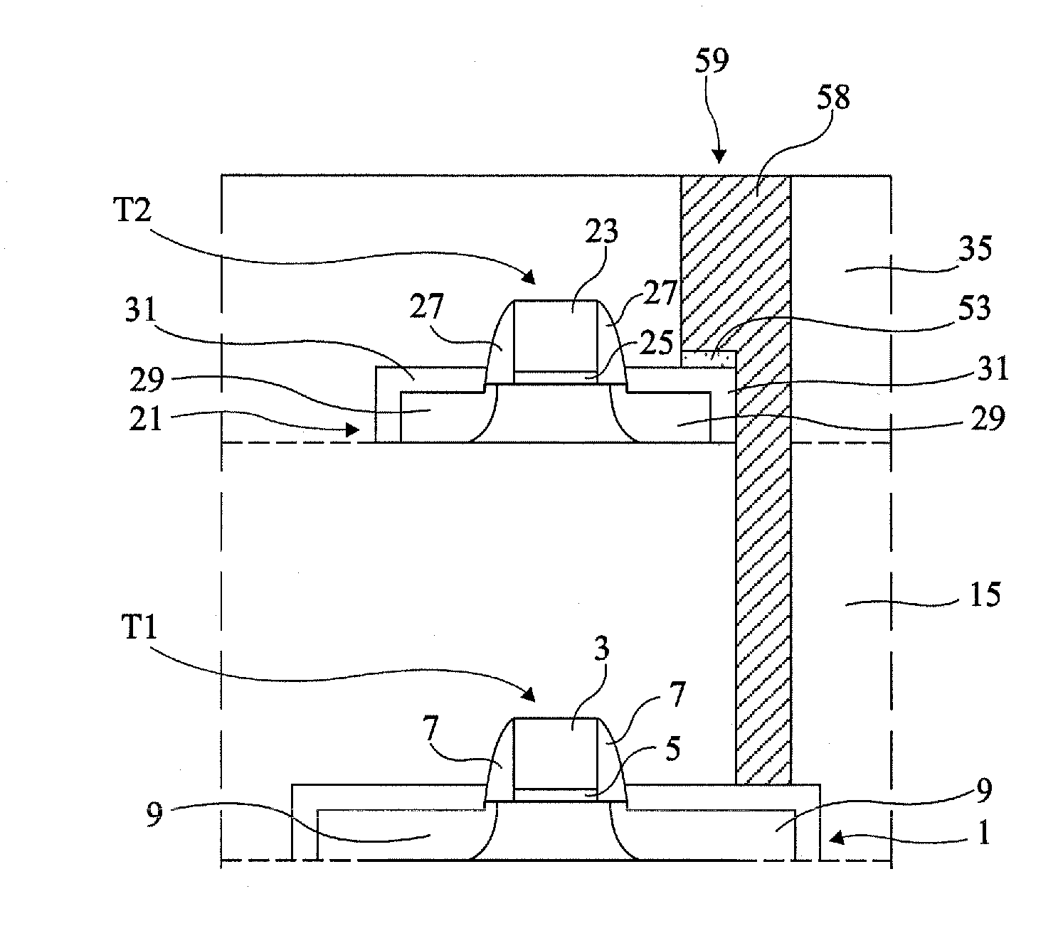
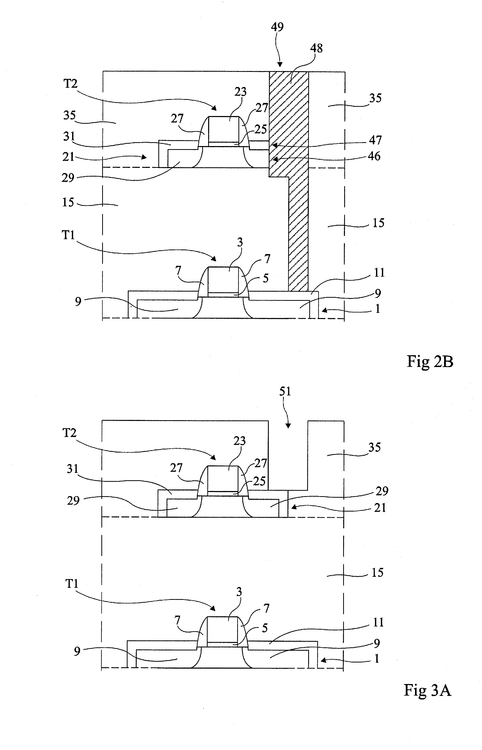
[0029]FIGS. 3A to 3D are cross-section views schematically illustrating successive steps of a method for forming a via contacting two levels of semiconductor layers.
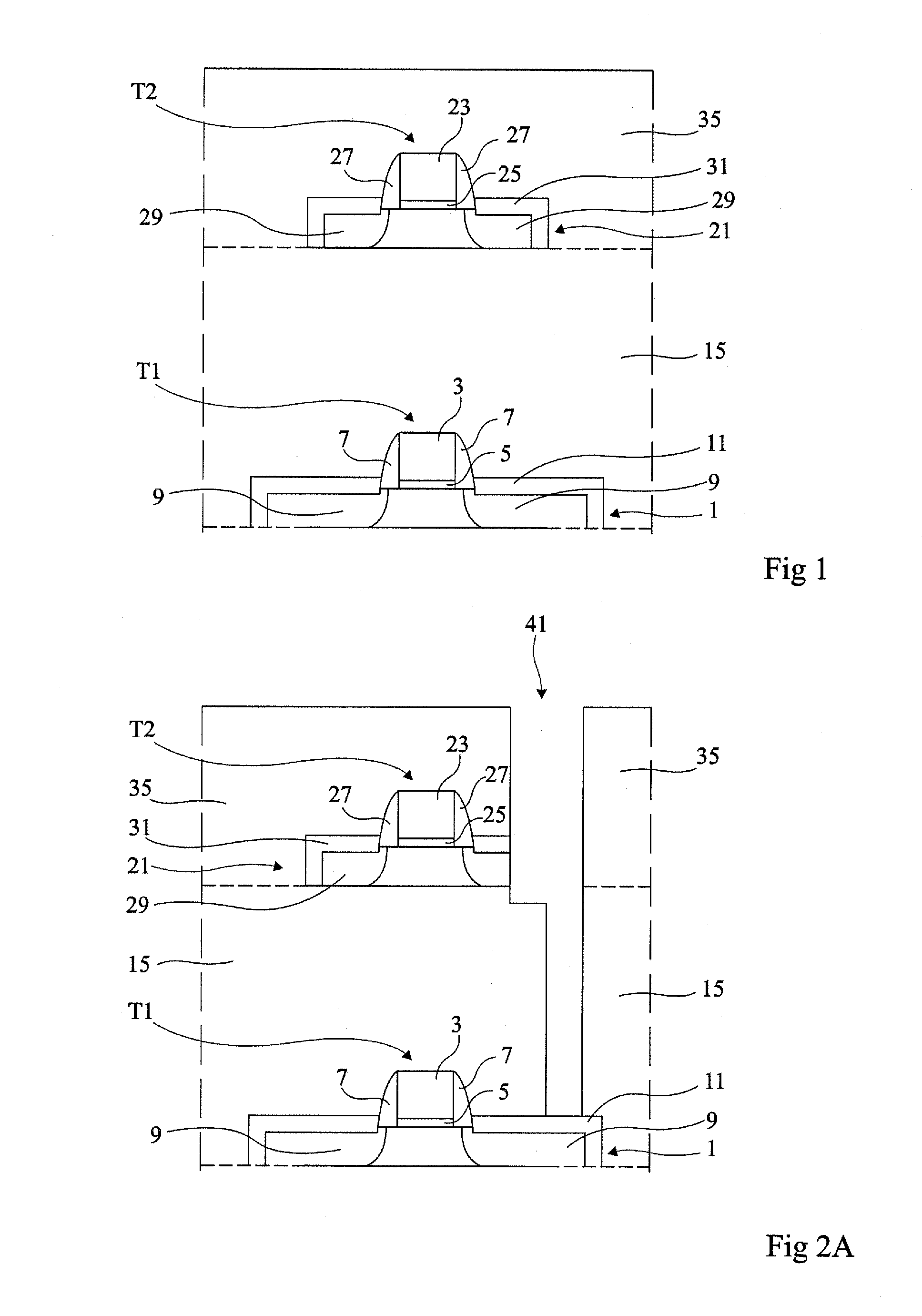
[0030]FIG. 3A shows a 3D structure of the type illustrated in FIG. 1 after the forming of an opening 51 to reach an edge of metal silicide layer 31 covering upper level silicon layer 21, opening 51 laterally continuing beyond the edge of layer 31. Before the forming of opening 51, a previous masking step has been carried out to protect the regions which are not desired to be etched. Opening 51 has been formed by an anisotropic etching method, for example, by plasma etching.
[0031]As an example of order of magnitude, the thickness of silicon layer 21 ranges between 5 and 150 nm, for example, on the order of 6 nm. Metal silicide layer 31 is for example based on platinum and / or nickel, and its thickness for example ranges between 5 and 30 nm, for example from 2 to 3 nm. Insulating layers 15 and 35 are for example made of sil...
PUM
 Abstract
Description
Claims
Application Information


