Array substrate and broken line repairing method

An array substrate and repair method technology, applied in nonlinear optics, instruments, optics, etc., can solve the problems of increasing panel size, affecting product yield, and lack of product competitiveness, and achieving the effect of improving product yield

Active Publication Date: 2019-04-26
SHENZHEN CHINA STAR OPTOELECTRONICS SEMICON DISPLAY TECH CO LTD
View PDF11 Cites 5 Cited by
  • Summary
  • Abstract
  • Description
  • Claims
  • Application Information

AI Technical Summary

Problems solved by technology

[0009] An embodiment of the present invention provides an array substrate, which is used to solve the problem that the transmittance of the pixel area of ​​the product is seriously reduced or the panel size of the product is increased due to the traditional disconnection repair method of the array substrate in the prior art, which affects the product. Quality, affecting product yield, resulting in technical problems of insufficient product competitiveness

Method used


Image

  • Array substrate and broken line repairing method
  • Array substrate and broken line repairing method
  • Array substrate and broken line repairing method

Examples


Embodiment Construction

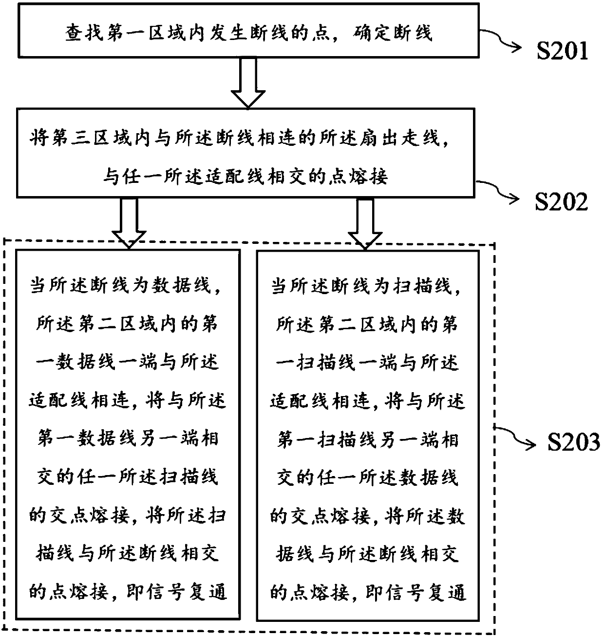
[0033] The following will clearly and completely describe the technical solutions in the embodiments of the present invention with reference to the accompanying drawings in the embodiments of the present invention. Obviously, the described embodiments are only some, not all, embodiments of the present invention. Based on the embodiments of the present invention, all other embodiments obtained by those skilled in the art without making creative efforts belong to the protection scope of the present invention.

[0034] Due to the use of the traditional disconnection repair method for the array substrate in the prior art, the transmittance of the pixel area of ​​the product is seriously reduced or the panel size of the product is increased, which affects product quality and product yield, resulting in insufficient product competitiveness , this embodiment can solve this defect.

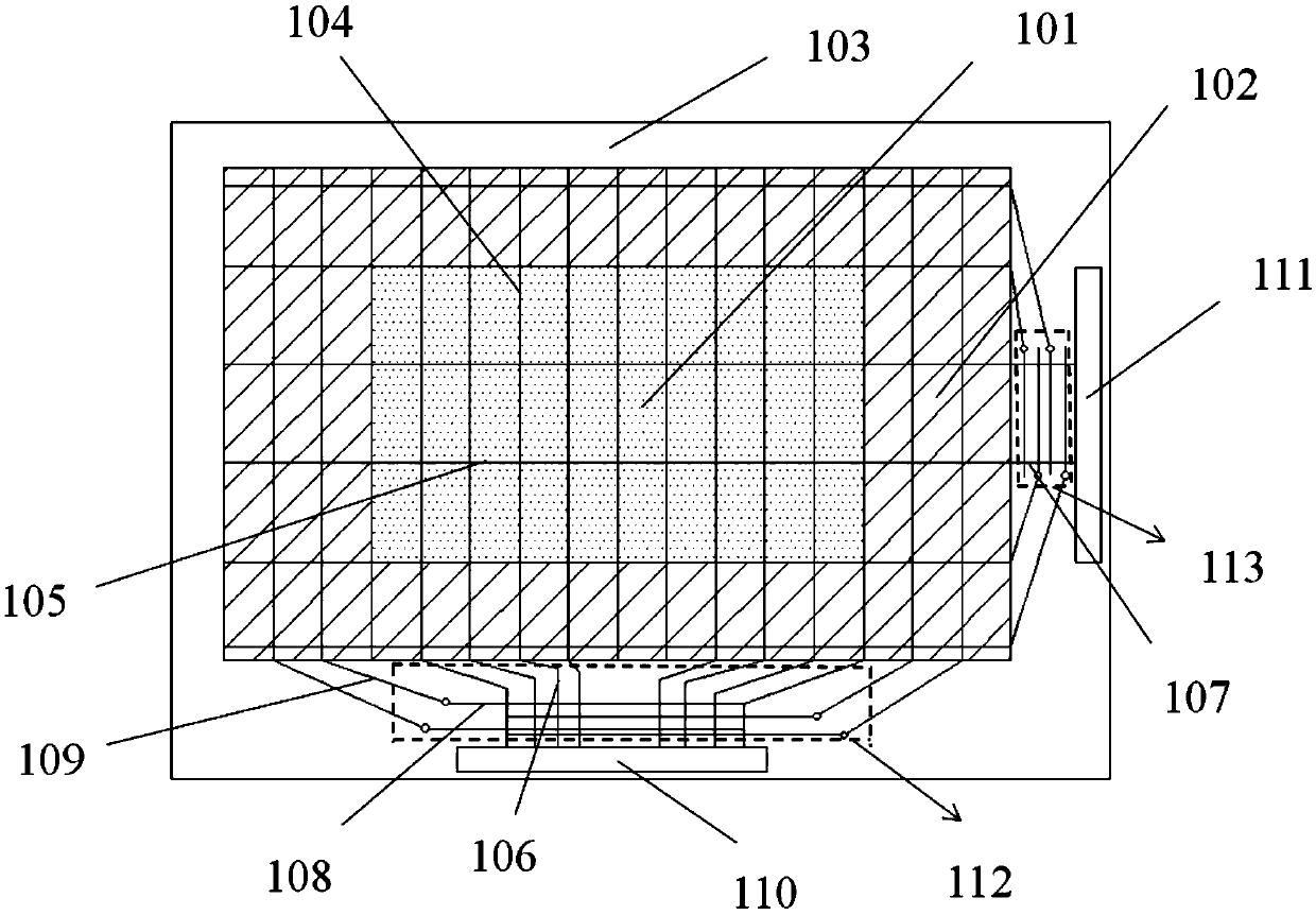
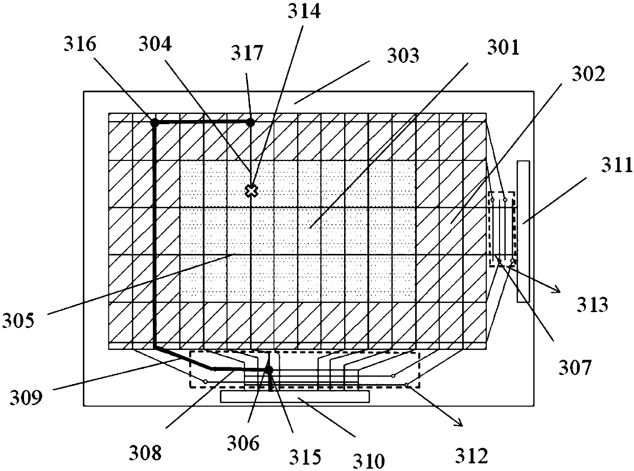
[0035] Such as figure 1 As shown, the structure schematic diagram of the array substrate provided by ...


PUM


Abstract

The invention provides an array substrate. The array substrate comprises a first area corresponding to a display area of a display panel, a second area which corresponds to a non-display area and is located on the outer side of the first area and a third area which corresponds to the non-display area and is located on the outer side the second area; the first area and the second area are providedwith at least two mutually parallel data lines, and at least two scanning lines perpendicular to the data lines; the third area is provided with a fan-out line and at least one adapter line intersecting with the fan-out line in different planes; the fan-out line is correspondingly connected with the data lines or the scanning lines of the first area; one ends of the adapter lines are connected with the data lines or the scanning lines of the second area, and the other ends of the adapter lines form breaking points. The array substrate has the advantages that by designing the multiple data lines and scanning lines, any broken lines in the panel can be repaired without lowering the transmittance of a pixel area or increasing the size of the panel.

Description

technical field [0001] The present invention relates to the field of display technology, in particular to an array substrate and a method for repairing disconnection thereof. Background technique [0002] TFT-LCD is very popular because of its high quality and low price, light weight, easy to carry, long service life, clear picture and high reliability. TFT-LCD products can be seen everywhere in our daily life, ranging from commercial advertisements to smart watches. Because of its high reliability, it is also widely used in military industries, such as aerospace and aviation. Although many advanced display modes have emerged, such as OLED, QD, LED, Micro-LED, ink screen, etc., due to various reasons such as cost, life, reliability, materials, and technical obstacles, they have not been able to replace TFT-LCD. status. TFT-LCD is still the current main force. [0003] With the improvement of people's living standards and the rapid development of science and technology, p...

Claims


Application Information

Patent Timeline
Patent Type & Authority Applications(China)
IPC IPC(8): G02F1/1362G02F1/1345
CPCG02F1/13452G02F1/136259G02F1/136263
Inventor 李柱辉
Owner SHENZHEN CHINA STAR OPTOELECTRONICS SEMICON DISPLAY TECH CO LTD
Why Eureka
Try Eureka