OLED display substrate, manufacturing method of OLED display substrate, display device
A technology of display substrate and display surface, applied in semiconductor devices, electrical components, circuits, etc., can solve problems such as the influence of the display effect of OLED display devices
- Summary
- Abstract
- Description
- Claims
- Application Information
AI Technical Summary
Problems solved by technology
Method used
Image

Examples
Embodiment 1
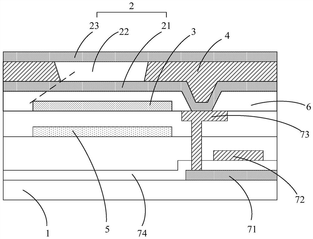
[0034] This embodiment provides an OLED display substrate, where most of the whole area of the OLED display substrate is a transparent area (specifically, the area of the OLED device 2 is a transparent area, and the area of the thin film transistor is a non-transparent area).
[0035] Such as figure 1 As shown, the OLED display substrate provided in this embodiment includes the following structure: a substrate 1 , and a plurality of OLED devices 2 and light selection patterns 3 disposed on the substrate 1 . in,
[0036] The substrate 1 is a transparent substrate 1, and its material may include materials such as polyimide, polyethylene terephthalate, polyethylene naphthalate, polycarbonate, and polyethersulfone.
[0037] The OLED device 2 includes: a transparent first electrode 21 , a light emitting layer 22 , and a transparent second electrode 23 sequentially disposed on the substrate 1 along a direction away from the substrate 1 . Wherein, the light emitting layer 22 ...
Embodiment 2
[0052] This embodiment provides a method for preparing an OLED display substrate, which can be used to prepare any OLED display substrate provided in Embodiment 1. The preparation method includes:
[0053] A step of forming a plurality of light selection patterns and a plurality of OLED devices on a substrate; wherein the OLED device includes: a transparent first electrode, a light-emitting layer, and a transparent second electrode; the light selection patterns are arranged on the non-display surface side of the OLED device , and one-to-one correspondence with the OLED devices; the wavelength range of the light allowed to pass by each light selection pattern is the same as the wavelength range of the light emitted by the corresponding OLED device.
[0054] And, in the step of forming the transflective structure on the side of the light selection pattern away from the OLED device, the reflectivity of the transflective structure to the light incident from the side close to the l...
Embodiment 3
[0080] This embodiment provides a display device, including any OLED display substrate provided in Embodiment 1.
[0081] Wherein, the display device may be a display device, such as a mobile phone, a tablet computer, a television, a monitor, a notebook computer, a digital photo frame, a navigator, and any other product or component with a display function.
PUM
| Property | Measurement | Unit |
|---|---|---|
| thickness | aaaaa | aaaaa |
| thickness | aaaaa | aaaaa |
Abstract
Description
Claims
Application Information
 - R&D
- Intellectual Property
- Life Sciences
- Materials
- Tech Scout
- Unparalleled Data Quality
- Higher Quality Content
- 60% Fewer Hallucinations
Browse by: Latest US Patents, China's latest patents, Technical Efficacy Thesaurus, Application Domain, Technology Topic, Popular Technical Reports.
© 2025 PatSnap. All rights reserved.Legal|Privacy policy|Modern Slavery Act Transparency Statement|Sitemap|About US| Contact US: help@patsnap.com