

OLED display panel, manufacturing method thereof and display device
A technology for display panels and manufacturing methods, applied in the field of OLED displays, capable of solving problems such as cracks and affecting packaging effects
- Summary
- Abstract
- Description
- Claims
- Application Information
AI Technical Summary
Problems solved by technology
Method used
Image

Examples
Embodiment 1
[0026] Embodiment 1 of the present invention proposes an OLED display panel, which includes:
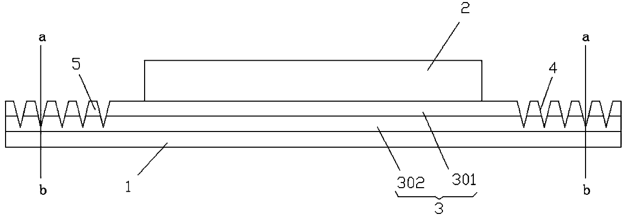
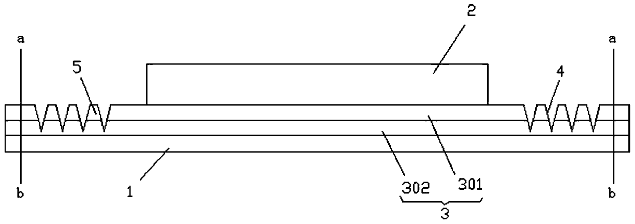
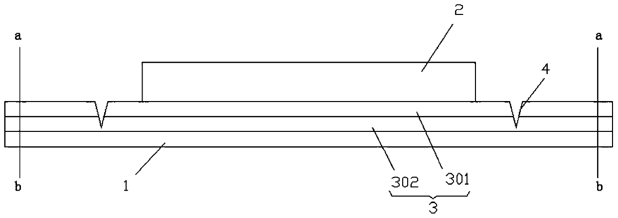
[0027] Such as Figure 1-Figure 5 As shown, the substrate 1, the protective layer 3 and the display function layer 2, the protective layer 2 is stacked on the substrate 1, and the protective layer 3 includes a first area and a second area surrounding the first area; the display function layer 2, the display function The layer 2 is arranged on the protected layer 3 and corresponds to the position of the first area; wherein, an annular groove 4 is arranged on the surface of the second area, and the annular groove 4 is arranged around the outside of the first area, and the annular groove 4 The bottom of the groove is pointed, which is used to prevent the second area from forming a gap that can extend to the first area.
[0028] Wherein, the substrate 1 is the base of the display panel and the supporting part of the device. The substrate 1 can be a flexible substrate in the prior art. F...
Embodiment 2
[0039] Such as Figure 6 As shown, Embodiment 2 of the present invention proposes a method for manufacturing an OLED display panel, the method comprising:
[0040] S1: Form a protective layer 3 on a substrate 1 .
[0041] Specifically, the protective layer 3 can completely cover the substrate 1 . The substrate 1 can be any substrate 1 in the prior art, for example, it can be a flexible substrate 1, and the material of the flexible substrate 1 can be a polymer substrate, an ultra-thin glass substrate, a stainless steel substrate, etc., which will not be described in detail here. limit.
[0042] S2: Setting display function 2 on the first area of protective layer 3 .
[0043] S3: Prepare the ring groove 4 on the second region of the protective layer 3 .
[0044] Specifically, the protective layer 3 and the display function 2 are successively formed on the substrate 1. The display function 2 includes organic materials and electrodes constituting the OLED device, etc., and t...
Embodiment 3
[0048] Embodiment 3 of the present invention proposes a display device, which includes:
[0049] A display device body and the aforementioned OLED display panel.
[0050] The display device body can be an electronic device with a display function such as a mobile phone, a computer, and a television in the prior art, and the above-mentioned OLED display panel is used.
[0051] The embodiment of the present invention proposes a display device. By setting the ring groove 4 in the second area of the protective layer and setting the groove bottom of the ring groove 4 as a sharp angle, when the edge of the display device body is hit, the collision along the The tip of the groove bottom of the ring groove 4 produces a gap perpendicular to the direction of the substrate 1, the gap will not extend to the packaging area, and the second area is a non-luminous area, which will not affect the display function of the display device body, and solves the problem of the prior art In this ca...
PUM
 Abstract
Description
Claims
Application Information