Touch panel and preparation method thereof

A touch panel and touch layer technology, applied in organic semiconductor devices, optics, instruments, etc., can solve the problems of sensor stripe cracks, cracks, excessive resistance and capacitance delay, etc., and achieve the effect of reducing delay effect and reducing cracks

Inactive Publication Date: 2019-07-23
SHENZHEN CHINA STAR OPTOELECTRONICS SEMICON DISPLAY TECH CO LTD
View PDF4 Cites 4 Cited by
  • Summary
  • Abstract
  • Description
  • Claims
  • Application Information

AI Technical Summary

Problems solved by technology

[0004] In the prior art liquid crystal cell products, In-Cell refers to the method of embedding the touch panel function into the liquid crystal pixel, that is, embedding the touch sensor function inside the display screen, making the touch panel relatively light and thin, and adopting a square touch sensor des

Method used


Image

  • Touch panel and preparation method thereof
  • Touch panel and preparation method thereof
  • Touch panel and preparation method thereof

Examples


Embodiment Construction

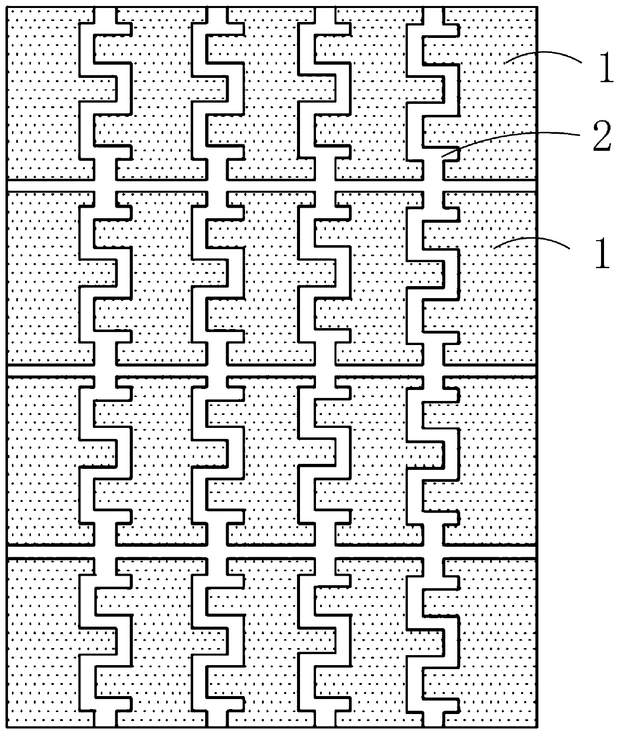
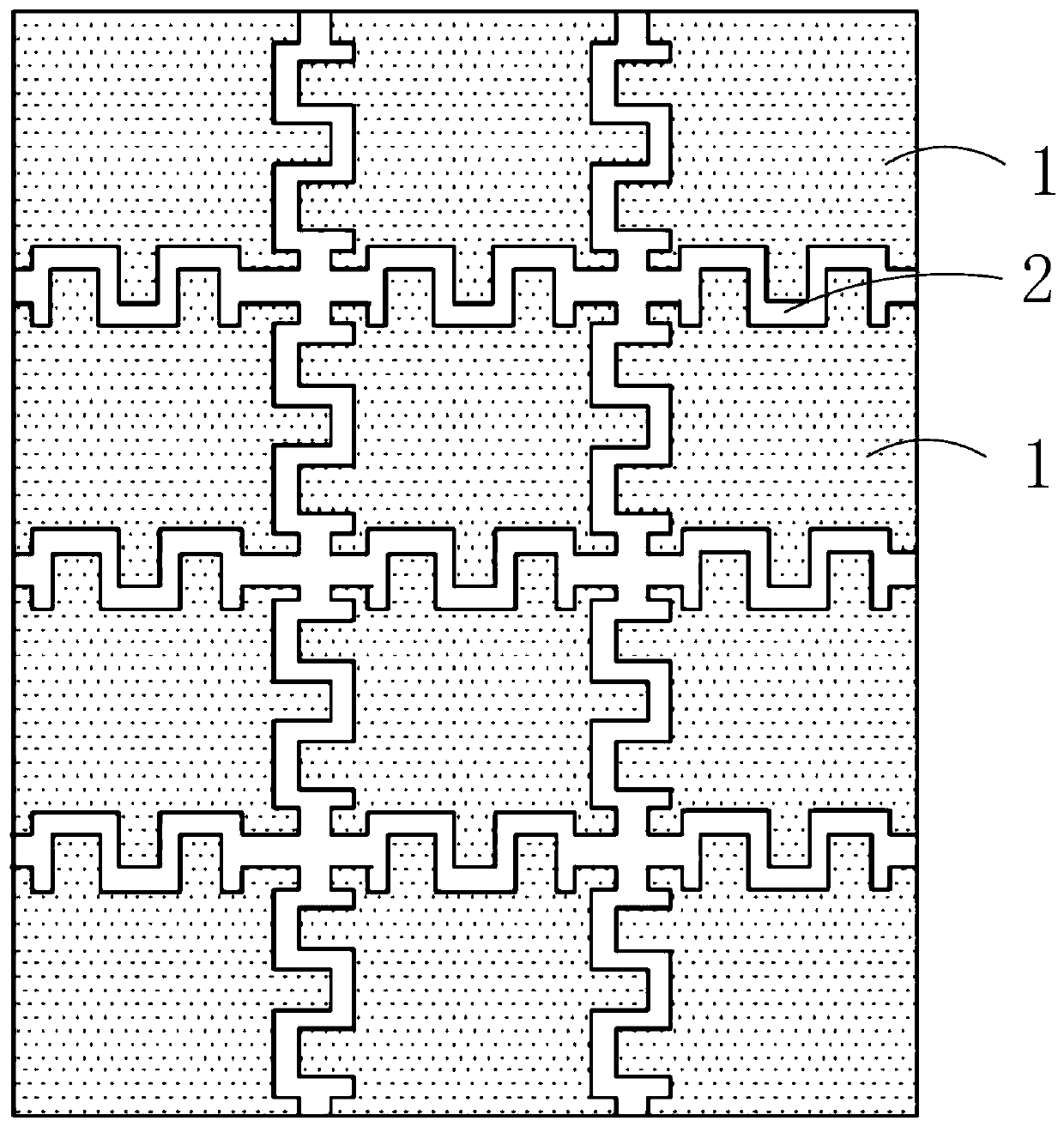
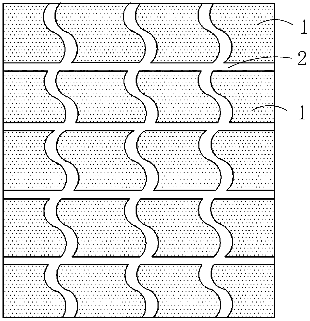
[0030] The following descriptions of the various embodiments refer to the accompanying drawings to illustrate specific embodiments in which the invention may be practiced. The directional terms mentioned in the present invention, such as [top], [bottom], [front], [back], [left], [right], [inside], [outside], [side], etc., are only for reference The orientation of the attached schema. Therefore, the directional terms used are used to illustrate and understand the present invention, but not to limit the present invention. In the figures, structurally similar elements are denoted by the same reference numerals.

[0031] In the description of the present application, it should be understood that the terms "center", "longitudinal", "transverse", "length", "width", "thickness", "upper", "lower", "front", " Orientation indicated by rear, left, right, vertical, horizontal, top, bottom, inside, outside, clockwise, counterclockwise, etc. The positional relationship is based on the or...


PUM

PropertyMeasurementUnit
Widthaaaaaaaaaa

Abstract

The invention provides a touch panel which comprises a substrate and a touch layer located on the substrate, the touch layer comprises a plurality of touch units arranged at intervals, an area betweenevery two adjacent touch units forms a lead area, and the lead areas are filled with lead materials;the edge of each touch unit is engaged with the edge of at least one adjacent touch unit, the touchpanel has the advantages that the graph of the touch unit inside the touch panel is made into a matched shape, the resistance-capacitance delay effect of the touch panel is reduced, and then the situation that the touch panel cracks is relieved.

Description

technical field [0001] The invention relates to the field of display technology, in particular to a touch panel and a preparation method thereof. Background technique [0002] With the development of large-size display applications, there are more and more demands for human-computer interaction, and touch applications have become an important medium in human-computer interaction. [0003] According to the position where the touch circuit is embedded in the liquid crystal display panel, the embedded touch panel can be divided into a touch circuit on the liquid crystal cell (On Cell) type and a touch circuit in the liquid crystal cell (In Cell) type. [0004] In the prior art liquid crystal cell products, In-Cell refers to the method of embedding the touch panel function into the liquid crystal pixel, that is, embedding the touch sensor function inside the display screen, making the touch panel relatively light and thin, and adopting a square touch sensor design, Since adjace...

Claims


Application Information

Patent Timeline
IPC IPC(8): G06F3/044G06F3/045H01L27/32G02F1/1333
CPCG06F3/044G06F3/045G02F1/13338G06F2203/04103H10K59/40H10K59/131H10K77/111H10K2102/311
Inventor 吴焕达
Owner SHENZHEN CHINA STAR OPTOELECTRONICS SEMICON DISPLAY TECH CO LTD
Why Eureka
Try Eureka