Semiconductor component 3D detector

A component and semiconductor technology, applied in the field of 3D testing machines for semiconductor components, can solve the problems of inconvenient transportation of semiconductor components, inconvenient adjustment, etc. Effect

Active Publication Date: 2019-10-15
江苏晶度半导体科技有限公司
View PDF11 Cites 1 Cited by
  • Summary
  • Abstract
  • Description
  • Claims
  • Application Information

AI Technical Summary

Problems solved by technology

[0004] The purpose of the present invention is to provide a 3D inspection machine for semiconductor components to solve the problems that the 3D inspection machine for semiconductor components proposed in the background art is inconvenient for the transportation of semiconductor components and the adjustment of the height and direction of the display screen

Method used


Image

  • Semiconductor component 3D detector
  • Semiconductor component 3D detector
  • Semiconductor component 3D detector

Examples


Embodiment 1

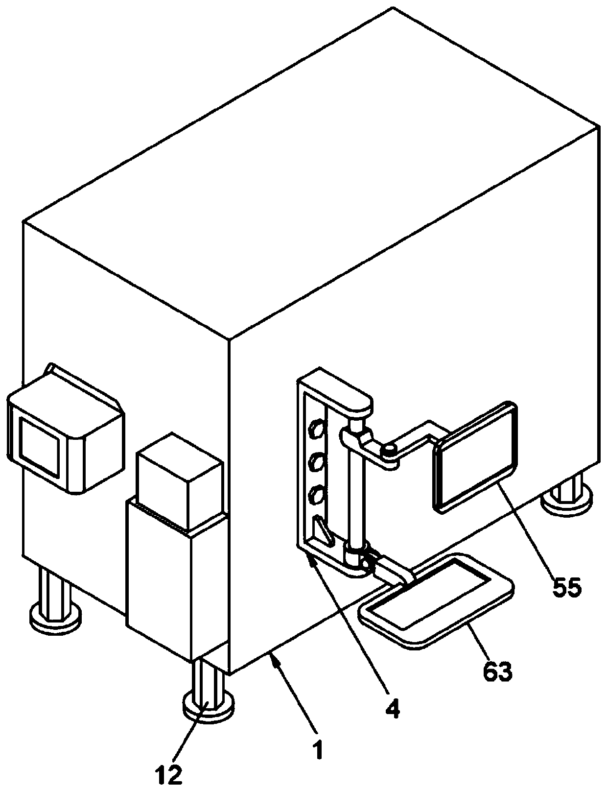
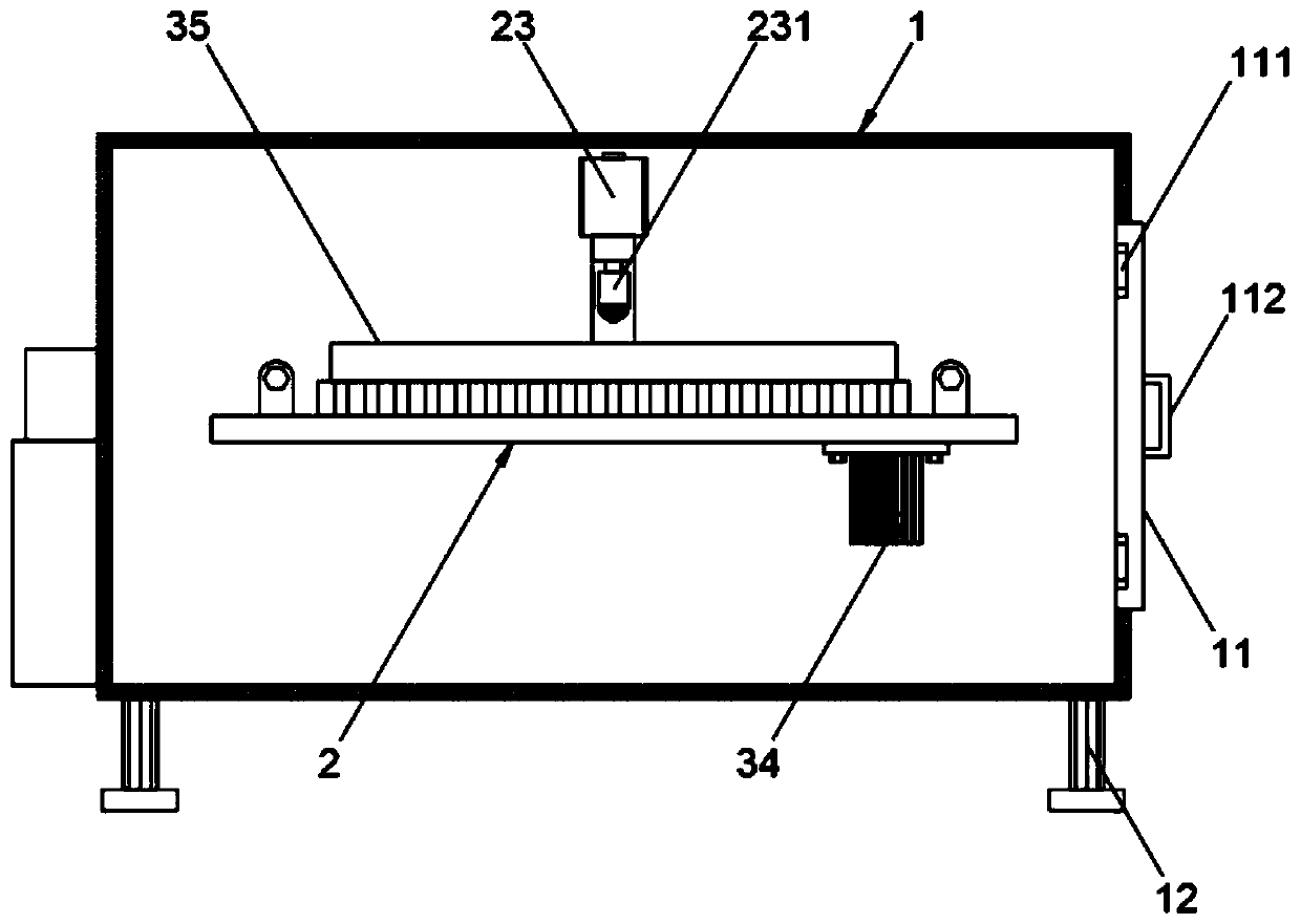
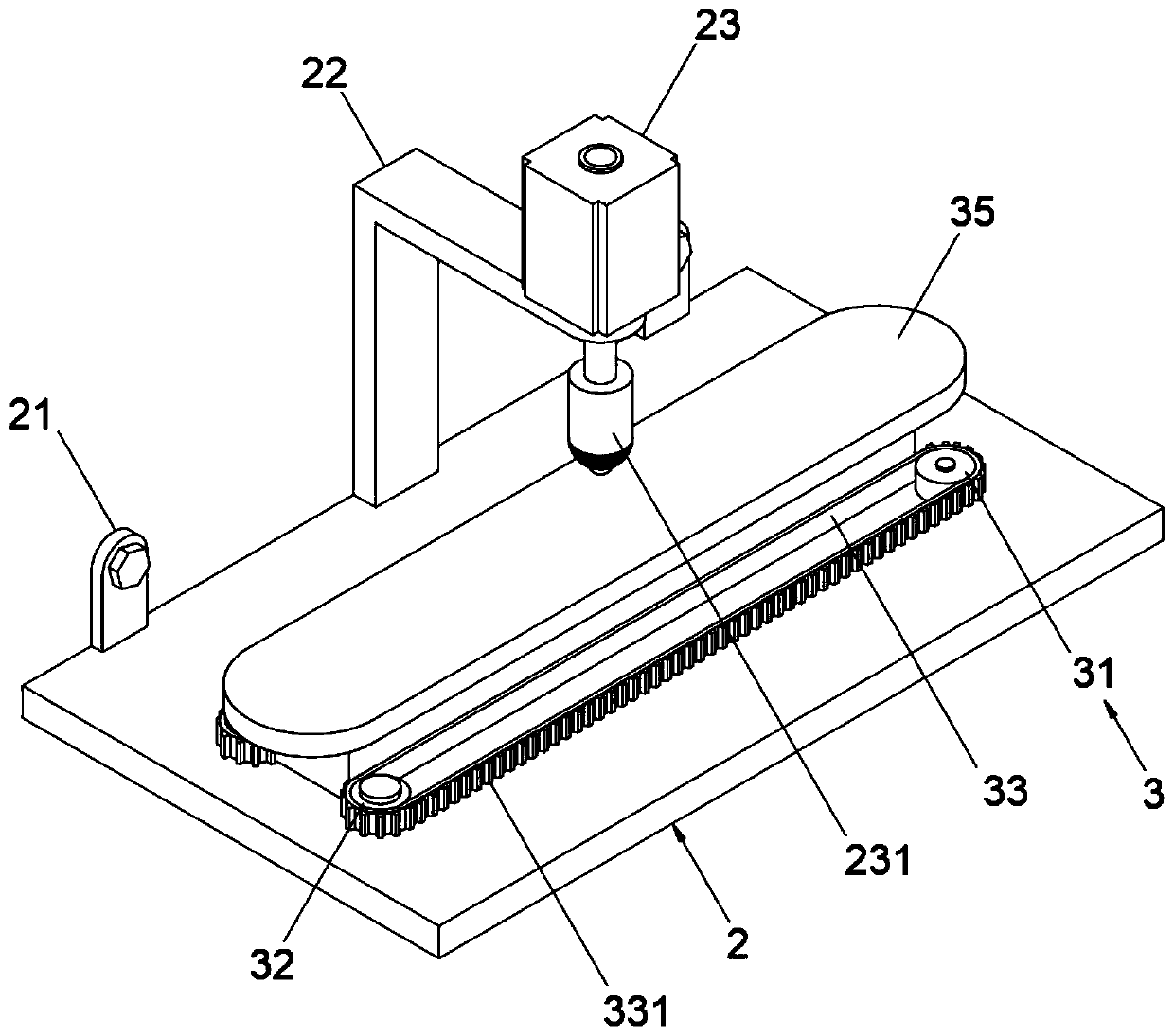
[0035] As a first embodiment of the present invention, a 3D inspection machine for semiconductor components, such as Figure 1-7Shown, comprise box body 1, the back surface of box body 1 is provided with box door 11, and box door 11 is provided with the joint of box body hinge 111, and box door 11 is hinged with box body 1 by hinge 111, and box body 1 There is a bottom plate 2 inside, and two fixing blocks 21 are tightly welded on one side of the bottom plate 2, and fixing bolts 211 are arranged on the fixing blocks 21, and the fixing blocks 21 are fixedly connected with the inner wall of the box body 1 through the fixing bolts 211, and the top of the bottom plate 2 The surface is provided with an L-shaped bracket 22, the vertical end of the L-shaped bracket 22 is tightly welded to the upper surface of the base plate 2, the horizontal end of the L-shaped bracket 22 is provided with a first through hole 221, and the L-shaped bracket 22 is equipped with a cylinder 23, A 3D camer...

Embodiment 2

[0042] As the second preferred embodiment of the present invention, the four corners of the lower surface of the box body 1 are provided with supporting feet 12, which is convenient to use the supporting feet 12 to support the box body 1, and prevent the bottom surface of the box body 1 from being damaged after being damp. corrosion.

Embodiment 3

[0044] As a third preferred embodiment of the present invention, a ring 341 is tightly welded on the motor 34, and first bolts 342 are arranged on both sides of the ring 341, and the ring 341 connects with the lower surface of the bottom plate 2 through the first bolt 342 For fixed connection, the lower surface of the bottom plate 2 is provided with a screw hole suitable for the first bolt 342 , so that the first bolt 342 is screwed into the screw hole, so as to facilitate fixing the motor 34 on the lower surface of the bottom plate 2 .


PUM


Abstract

The invention relates to the technical field of semiconductor equipment, and in particular relates to a semiconductor component 3D detector, comprising a box in which a base plate is arranged in the box; two transmission devices are arranged on the upper surface of the base plate; a U-shaped support is arranged on the front surface of the box; a support rod is arranged between the two horizontal ends of the U-shaped support; an adjustment base is arranged on the top end of the support rod; and a lantern ring is arranged at the bottom end of the support rod. According to the semiconductor component 3D detector provided by the invention, the transmission device is arranged on the base plate in the box, so that the semiconductor component is convenient to transmit for detection, and the detection accuracy is improved; in addition, the U-shaped support is installed on the front surface of the box, the support rod is arranged on the U-shaped support; the support rod penetrates through a through hole in the adjustment base; through moving the support rod up and down in the through hole, the height of the adjustment base is convenient to fix; a support frame rotates via a second rotationshaft, so that the turning of the display screen is convenient to adjust, and the problem that the semiconductor component 3D detector is inconvenient to transmit the semiconductor component and inconvenient to adjust the height and turning of the display screen is solved.

Description

technical field [0001] The invention relates to the technical field of semiconductor equipment, in particular to a 3D inspection machine for semiconductor components. Background technique [0002] A semiconductor is a material whose electrical conductivity is between that of a conductor and an insulator at room temperature. Semiconductors have a wide range of applications in radios, televisions, and temperature measurement. For example, a diode is a device made of a semiconductor. A semiconductor is a material whose electrical conductivity can be controlled, ranging from an insulator to a conductor. No matter from the perspective of technology or economic development, the importance of semiconductors is huge. The core units of most of today's electronic products, such as computers, mobile phones or digital recorders, are closely related to semiconductors. [0003] At present, in the production process of semiconductors, it is necessary to carry out 3D inspection on semic...

Claims


Application Information

Patent Timeline
Patent Type & Authority Applications(China)
IPC IPC(8): G01N21/89G01N21/13G01N21/01
CPCG01N21/89G01N21/13G01N21/01G01N2021/0112G01N2021/0162
Inventor 凌永康杜良辉孙国标
Owner 江苏晶度半导体科技有限公司
Why Eureka
Try Eureka