
A self-sealing micro-nanofluidic chip processing method

A technology of micro-nano fluidic control and processing method, which is applied in the direction of chemical instruments and methods, laboratory containers, laboratory utensils, etc., which can solve the problems of unstable structure, small amount of liquid sample and airtightness, etc., and achieve good airtightness Good sealing performance and high structural precision

Active Publication Date: 2021-09-24
杭州欧光芯科技有限公司
View PDF6 Cites 0 Cited by
  • Summary
  • Abstract
  • Description
  • Claims
  • Application Information

AI Technical Summary

Problems solved by technology

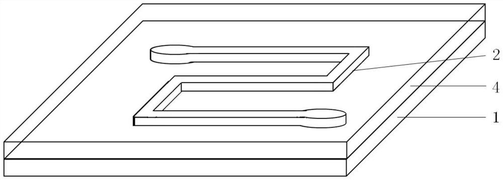
[0005] In order to solve the problems existing in the background technology, the present invention proposes a self-sealing micro-nanofluidic chip processing method, which solves the problem of sealing performance and structural instability of the micro-nanofluidic chip with a small amount of liquid sample

Method used


Image

  • A self-sealing micro-nanofluidic chip processing method
  • A self-sealing micro-nanofluidic chip processing method
  • A self-sealing micro-nanofluidic chip processing method

Examples


Embodiment 1

[0031] To make a self-sealing nanofluidic chip by using the method described in the present invention, the specific steps are as follows:

[0032] 1. Spin-coat a layer of embossing glue on a 6-inch glass wafer, press the existing mold into the embossing glue with nano-imprinting equipment, and the embossing glue is cured after ultraviolet exposure, and then the mold and the cured embossing glue are combined Printing glue separation. In this way, the negative structure on the mold is transferred to the embossing glue, forming the desired nano-flow channel structure composed of the imprinting glue.

[0033] The specific parameters are as follows:

[0034] Spin coating revolutions of embossing glue 5000 rpm Imprint adhesive spin coating time 40 seconds UV exposure time 30 seconds

[0035] 2. Remove the residual layer of imprinting glue by reactive ion etching (RIE).

[0036] The specific parameters are as follows:

[0037] BCl3 gas flow...

Embodiment 2

[0046] A self-sealing microfluidic chip is manufactured by the method of the present invention, and the specific steps are as follows:

[0047] 1. Spin-coat a layer of photoresist on a 6-inch glass wafer, and expose it on a photolithography machine through a photolithography plate. There are patterns of micro-channels on the photolithography plate, and the pattern is opaque and other places are light-transmitting. The glass with photoresist is rinsed in the developer solution, and the photoresist is washed away in the exposed place, leaving only the microchannel structure composed of photoresist.

[0048] The specific parameters are as follows:

[0049] Photoresist spin coating revolutions 3000 rpm Photoresist Spin Time 40 seconds UV exposure time 10 seconds

[0050] 2. Use plasma stripping to remove residual glue.

[0051] The specific parameters are as follows:

[0052] Oxygen flow rate 100 sccm Nitrogen flow rate 30 sccm ...


PUM


Abstract

The invention discloses a self-sealing micro-nano fluidic chip processing method. On the substrate of glass or silicon wafer, use the method of nanoimprint to make the micro-nano channel composed of imprint glue and the residual layer on it, and the micro-nano channel also contains the residual layer; use the method of reactive ion etching Remove the residual layer of imprinting glue; use atomic layer deposition to deposit a layer of silicon dioxide SiO on the substrate and micro-nano flow channels 2 or titanium dioxide TiO 2 The deposition layer; punch holes at both ends of the micro-nano flow channel as the inlet and outlet of the liquid sample; put the substrate into a high-temperature heating furnace to heat, so that the imprinting glue is vaporized and volatilized. After the imprinting glue is completely volatilized, Take out the substrate to obtain the chip. The invention makes silicon dioxide or titanium dioxide and glass or silicon substrate closely combined to achieve excellent sealing, can realize the processing of micron-level or even nano-level high-precision structures, and can avoid high-temperature deformation and structural collapse of glass .

Description

technical field [0001] The invention relates to the field of micro-nano fluidic chips, in particular to a self-sealing micro-nano fluidic chip processing method. Background technique [0002] Micro-nanofluidic chip technology is a technology that integrates basic operations such as sample preparation, reaction, separation, and detection in the process of biological, chemical, and medical analysis into a chip with micron or nanoscale flow channels, and automatically completes the analysis. In recent years, with the breakthroughs in material science and micro-nano processing technology, micro-nanofluidic chips have also developed rapidly and their applications have become more and more extensive. At present, micro-nanofluidic chips have been used in many fields such as gene and protein sequencing, disease diagnosis, drug screening, etc., and have gradually become an important technical basis for systems biology, especially systems genetics. [0003] The amount of liquid sampl...

Claims


Application Information

Patent Timeline
Patent Type & Authority Patents(China)
IPC IPC(8): B01L3/00
CPCB01L3/502707B01L2300/12
Inventor 张琬皎
Owner 杭州欧光芯科技有限公司
Learn More