A kind of semiconductor wafer flattening equipment

A flattening and semiconductor technology, applied in the field of semiconductor wafer flattening equipment, can solve the problems of reducing wafer usage rate, easy scratching of wafer carrier, easy collapse of wafer carrier surface, etc., to achieve the effect of avoiding damage

Active Publication Date: 2021-04-02
江苏圣创半导体科技有限公司
View PDF6 Cites 0 Cited by
  • Summary
  • Abstract
  • Description
  • Claims
  • Application Information

AI Technical Summary

Problems solved by technology

[0003] After the surface-to-face contact between the grinding tool and the carrier, the surface of the wafer carrier is easily collapsed after the tool passes through, causing small or powdery particles to fly out. At present, it is rinsed with the grinding liquid and the grinding work is carried out at the same time. , but in the process of tool rotation, there is a certain amount of rotational traction and it is easy to involve waste materials, because most of the waste materials are polygonal, and it is easy to scratch the surface of the wafer carrier during the rotation of the tool, thus affecting the surface flatness of the wafer carrier , reducing wafer utilization

Method used


Image

  • A kind of semiconductor wafer flattening equipment
  • A kind of semiconductor wafer flattening equipment
  • A kind of semiconductor wafer flattening equipment

Examples


Embodiment

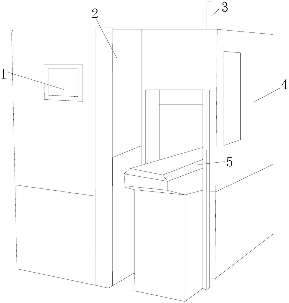
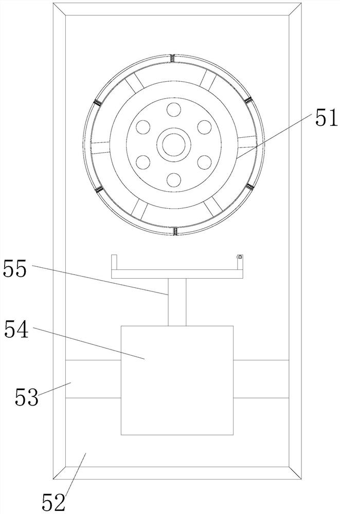
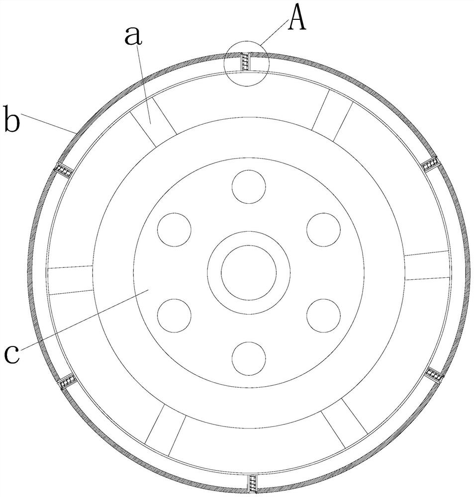
[0026] see Figure 1-Figure 7, the present invention provides a semiconductor wafer flattening equipment, the structure of which includes a control board 1, a device housing 2, a signal light 3, a working cabin 4, and a flat grinding device 5, wherein the flat grinding device 5 is located in the working cabin 4. The lower end of one side of the signal lamp 3 is provided and embedded in the interior of the working cabin 4. The two are fixedly connected by mechanical welding. The signal lamp 3 is perpendicular to the upper surface of the working cabin 4 and is movably connected with the working cabin 4. The device housing 2 and the working cabin 4 are an integrated structure connecting left and right, the device housing 2 is a rectangular block structure, and an embedded control panel 1 is provided on the front end of the device housing 2, and the flat grinding device 5 is provided with Grinding wheel device 51, mounting plate 52, chute 53, hydraulic cylinder 54, fixed frame 55,...


PUM


Abstract

The invention discloses a semiconductor wafer flattening device, the structure of which comprises a control panel, a device housing, a signal lamp, a working cabin, and a flat grinding device, and is characterized in that the flat grinding device is located at the lower end of the side of the working cabin where the signal light is provided And embedded in the working cabin, the two are fixedly connected by mechanical welding. The signal light is perpendicular to the upper surface of the working cabin and is movably connected with the working cabin. The device shell and the working cabin are an integrated structure connected left and right. The beneficial effects of the present invention are: Through the cooperation of the cleaner and the limiter, the arc-shaped column creates the movement trend of the flowing water, and cooperates with the flow-stopping effect provided by the wheel disc of the spiral plate body connected from head to tail to collect waste materials, and at the same time, the upper shape can be changed into a cushion The block is deformed under pressure and the fluff layer structure arranged horizontally to hook the remaining waste, enter the inside of the feed rack, and cycle back and forth, so as not to leave waste flying out on the surface to be ground, and to ensure the flatness control of the wafer to a great extent.

Description

technical field [0001] The invention relates to the field of semiconductors, in particular to a semiconductor wafer flattening device. Background technique [0002] Wafer refers to the silicon wafer used in the production of silicon semiconductor integrated circuits. During the processing, a variety of processing techniques are required to achieve the purpose of use. The flatness control of the wafer is processed by mechanochemical grinding. The flatness is very important for the use of finished products. The current semiconductor wafer planarization equipment usually uses vertical downward pressure to match the flat grinding tool when performing the planarization process. Rotation is powered for grinding work, but has the following drawbacks: [0003] After the surface-to-face contact between the grinding tool and the carrier, the surface of the wafer carrier is easily collapsed after the tool passes through, causing small or powdery particles to fly out. At present, it is...

Claims


Application Information

Patent Timeline
Patent Type & Authority Patents(China)
IPC IPC(8): B24B53/017
CPCB24B53/017
Inventor 陈珊邓筑蓉
Owner 江苏圣创半导体科技有限公司
Why Eureka
Try Eureka