Electronic component packaging structure and packaging method

A technology of electronic components and packaging structure, applied in the field of electronic component packaging structure and packaging, can solve problems such as packaging stress mismatch, failure, chip damage, etc.

Pending Publication Date: 2020-01-21
EDGELESS SEMICON CO LTD OF ZHUHAI +1
View PDF0 Cites 0 Cited by
  • Summary
  • Abstract
  • Description
  • Claims
  • Application Information

AI Technical Summary

Problems solved by technology

[0005] The purpose of the present invention is to provide an electronic component packaging structure and packaging method to solve the technical problem of chip damage and failure caused by packaging stress mismatch between the packaging protection layer and the chip existing in the prior art

Method used


Image

  • Electronic component packaging structure and packaging method
  • Electronic component packaging structure and packaging method
  • Electronic component packaging structure and packaging method

Examples


Embodiment Construction

[0045] In order to make the purpose, technical solution and advantages of the present invention clearer, the technical solution of the present invention will be described in detail below. Apparently, the described embodiments are only some of the embodiments of the present invention, but not all of them. Based on the embodiments of the present invention, all other implementations obtained by persons of ordinary skill in the art without making creative efforts fall within the protection scope of the present invention.

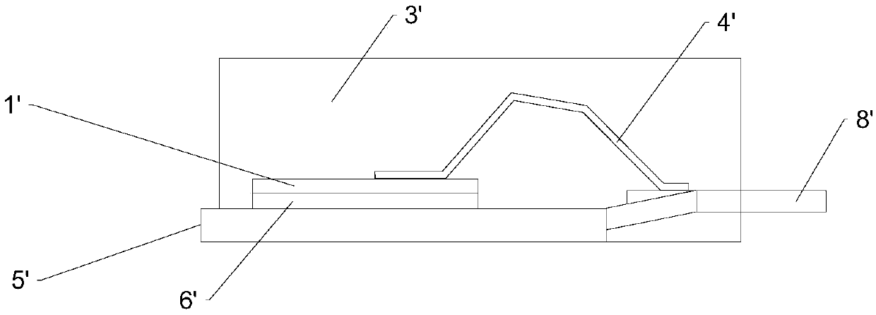
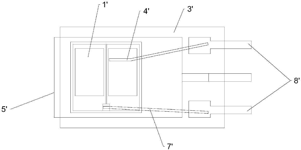
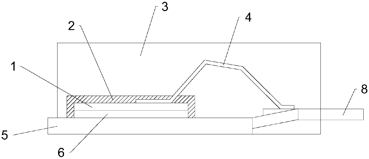
[0046] Such as image 3 and Figure 4 As shown, the present invention provides an electronic component packaging structure, including electronic components, a protective layer and a stress buffer layer, the stress buffer layer is between the electronic component and the protective layer, and the stress buffer layer can buffer and weaken the impact of the protective layer on the electron Package stress applied by components.

[0047] By arranging a stress buff...


PUM

PropertyMeasurementUnit
thicknessaaaaaaaaaa
thicknessaaaaaaaaaa
water absorptionaaaaaaaaaa

Abstract

The invention provides an electronic component packaging structure and a packaging method, and relates to the semiconductor device technology field. Technical problems of chip damages and failure caused by mismatching of a packaging stress between a packaging protection layer and a chip in the prior art are solved. The packaging structure comprises an electronic component, a protection layer and astress buffer layer. The stress buffer layer is arranged between the electronic component and the protection layer, and the stress buffer layer can buffer and weaken the packaging stress applied to the electronic component by the protection layer. The stress buffer layer is arranged between the electronic component and the protection layer to buffer and weaken the packaging stress applied to theelectronic component by the protection layer, a failure damage of the electronic component is reduced, water vapor invasion is prevented, ion pollution is isolated and reliability of the electronic component is improved.

Description

technical field [0001] The invention relates to the technical field of semiconductor devices, in particular to an electronic component packaging structure and packaging method. Background technique [0002] Packaging refers to connecting the circuit pins on the silicon chip to external connectors with wires so as to connect with other devices. Package form refers to the housing used to install semiconductor integrated circuit chips. It not only plays the role of installing, fixing, sealing, protecting the chip and enhancing the electrothermal performance, but also connects the contacts on the chip to the pins of the package shell with wires, and these pins pass through the wires on the printed circuit board. Connect with other devices to realize the connection between the internal chip and the external circuit. Because the chip must be isolated from the outside world to prevent impurities in the air from corroding the chip circuit and causing electrical performance degrada...

Claims


Application Information

Patent Timeline
Patent Type & Authority Applications(China)
IPC IPC(8): H01L23/00H01L21/56
CPCH01L23/562H01L21/56H01L2224/48472H01L2224/0603H01L2224/8592H01L2224/48095H01L2224/32245H01L2224/73265H01L2224/48247H01L2924/181H01L2924/00012
Inventor 曹俊江伟何昌
Owner EDGELESS SEMICON CO LTD OF ZHUHAI
Why Eureka
Try Eureka