Chip-on-chip film and display device

A technology for display devices and chip-on-chip films, which is applied in the direction of identification devices and instruments, and can solve problems such as abnormal display panel functions, misplaced connections between output pins and binding pads, etc.

Active Publication Date: 2021-07-06
TCL CHINA STAR OPTOELECTRONICS TECH CO LTD
View PDF30 Cites 0 Cited by
  • Summary
  • Abstract
  • Description
  • Claims
  • Application Information

AI Technical Summary

Problems solved by technology

In the bonding process of the chip-on-chip film and the display panel, it has always been a difficult problem in this field to ensure the accurate alignment of the output pins and the bonding pads. It is inevitable that the display panel will be thermally expanded to cause changes in the spacing of the output pins. If there is a deviation during the alignment process, it is easy to have a misaligned connection between the output pins and the binding pad, which will lead to abnormal function of the display panel.

Method used


Image

  • Chip-on-chip film and display device
  • Chip-on-chip film and display device
  • Chip-on-chip film and display device

Examples


Embodiment Construction

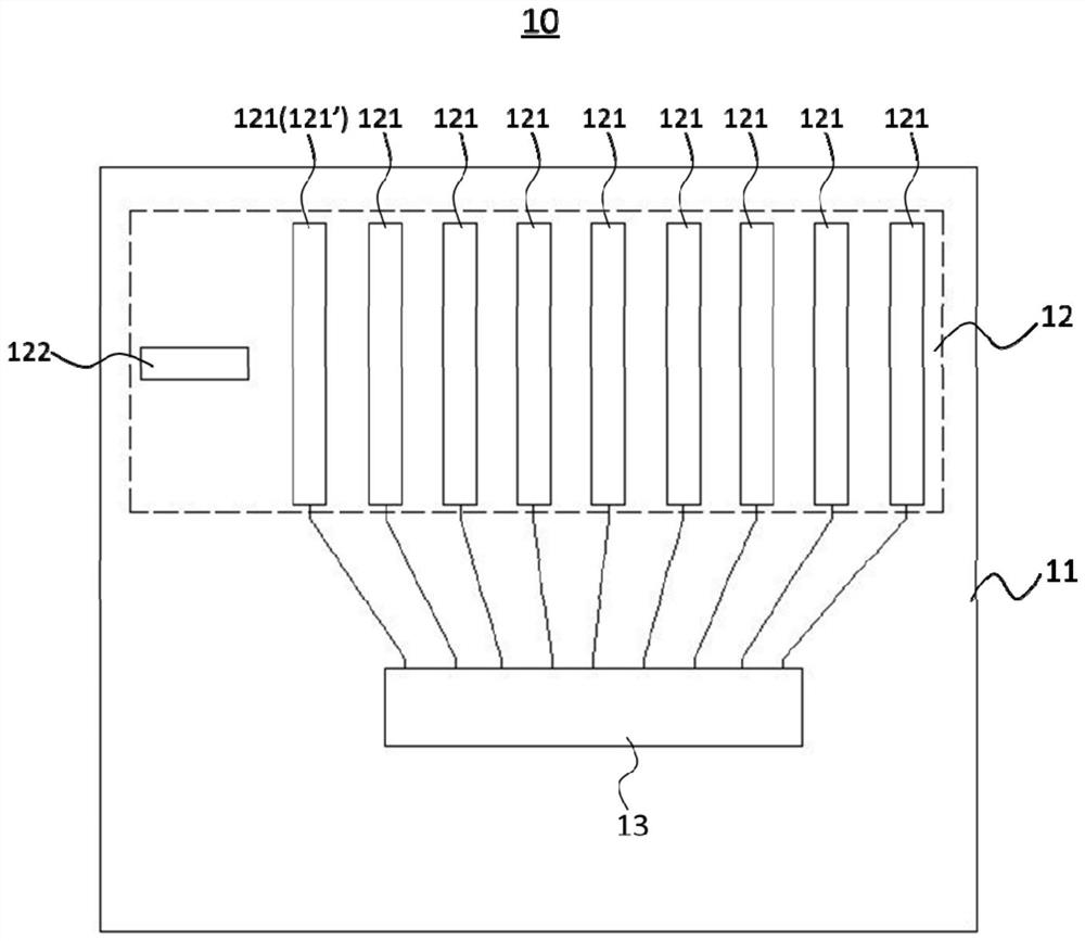
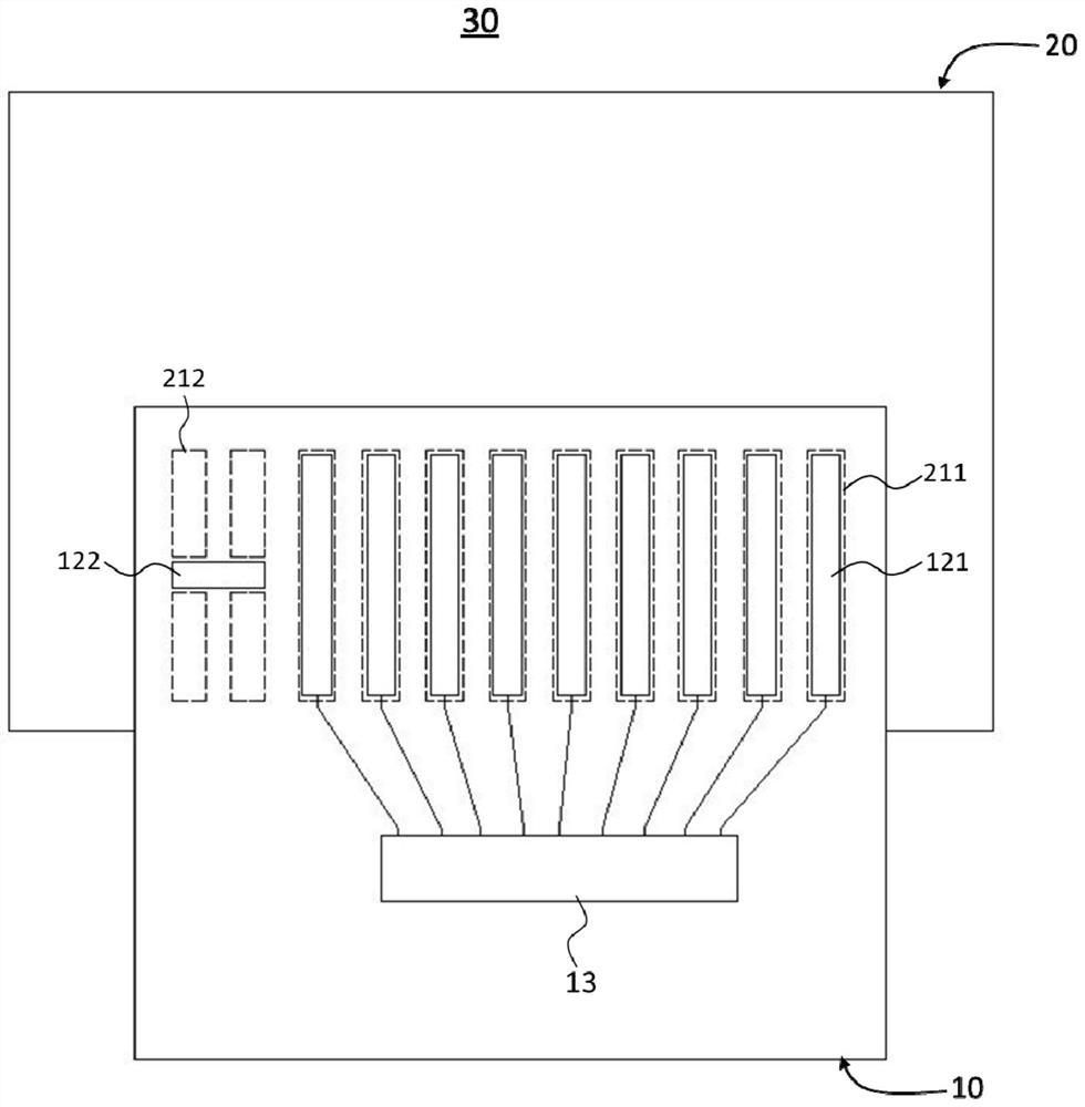
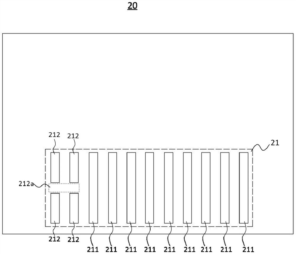
[0024] The following descriptions of the various embodiments refer to the accompanying drawings to illustrate specific embodiments in which the invention may be practiced. The directional terms mentioned in the present invention, such as [top], [bottom], [front], [back], [left], [right], [inside], [outside], [side], etc., are only for reference The orientation of the attached schema. Therefore, the directional terms used are used to illustrate and understand the present invention, but not to limit the present invention. In the figures, structurally similar elements are denoted by the same reference numerals.

[0025] An embodiment of the present invention provides a chip-on-film, by setting horizontal pins disconnected from the longitudinal pins on the side of the longitudinal pins of the chip-on-film, and implementing the chip-on-film through the horizontal pins Accurate alignment with the display panel solves the problem of difficult alignment in the bonding process of the...


PUM


Abstract

The present invention provides a chip-on-chip film and a display device. The chip-on-chip film includes a substrate, longitudinal pins for binding connection and horizontal pins for alignment, which are arranged on the substrate, and the The vertical pins are disconnected and insulated from the horizontal pins; the display device includes the above-mentioned chip-on-chip film and a display panel, and the display panel has binding pads and alignment pads, and the alignment pads are provided with alignment pads. Notches, the transverse pins are arranged in the alignment notches, and the binding pads are bound and connected with the longitudinal pins in alignment. The chip-on-chip film and the display device provided by the invention can realize the accurate alignment connection of the two, and improve the yield and reliability of production.

Description

technical field [0001] The invention relates to the field of display technology, in particular to a chip-on-chip film and a display device. Background technique [0002] With the development of display technology, especially the popularity of handheld display devices such as mobile phones and tablet computers, users have higher and higher requirements for product resolution. High resolution means higher wiring density under the same size. The higher the accuracy requirements of the bonding process. [0003] In the prior art, the control of the display function of the display panel by the driver chip is realized by binding and connecting a Chip on Film (COF) carrying the driver chip to an input terminal of the display panel. Therefore, output pins are provided on the COF, and binding pads correspondingly connected to the output pins are provided on the display panel. In the bonding process of the chip-on-chip film and the display panel, it has always been a difficult proble...

Claims


Application Information

Patent Timeline
Patent Type & Authority Patents(China)
IPC IPC(8): G09F9/00
CPCG09F9/00
Inventor 李继龙王月
Owner TCL CHINA STAR OPTOELECTRONICS TECH CO LTD
Why Eureka
Try Eureka