

Solid-Stated Image Pickup Device And Method For Manufacturing Same
a solid-state image and pickup device technology, applied in the direction of color television, television system, radio control device, etc., can solve the problems of insufficient adhesion, weakening the joining strength, and long-term reliability, so as to ensure the reliability of long-term devices, increase production yield, and reduce manufacturing costs.
- Summary
- Abstract
- Description
- Claims
- Application Information
AI Technical Summary
Benefits of technology
Problems solved by technology
Method used
Image

Examples
first embodiment
About Basic Configuration of Image Pickup Device
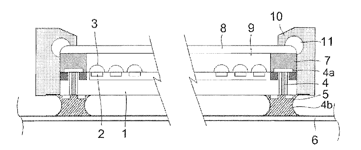
[0062]FIG. 1 is a configuration sectional view showing a first basic configuration of an image pickup device according to the present invention. The image pickup device is composed of an image sensor and an optical element and is formed by joining them with joining means such as adhesive. The image sensor is composed of a large number of light-receiving portions and semiconductor devices which bear an image pickup function such as an electrode, a wire, and a protection diode, and the optical element is composed of optical glass, a microlens, and the like. In the image pickup device, a transparent plate is joined to an upper portion of the image sensor with adhesive and is hermetically sealed.
[0063] An image pickup device shown in FIG. 1 has a large number of light-receiving portions 2 formed at a surface portion of a wafer 1 and a microlens 3 formed for each of the light-receiving portions 2. Through electrodes 4 are provided all ove...
second embodiment
About Method for Manufacturing Image Pickup Device
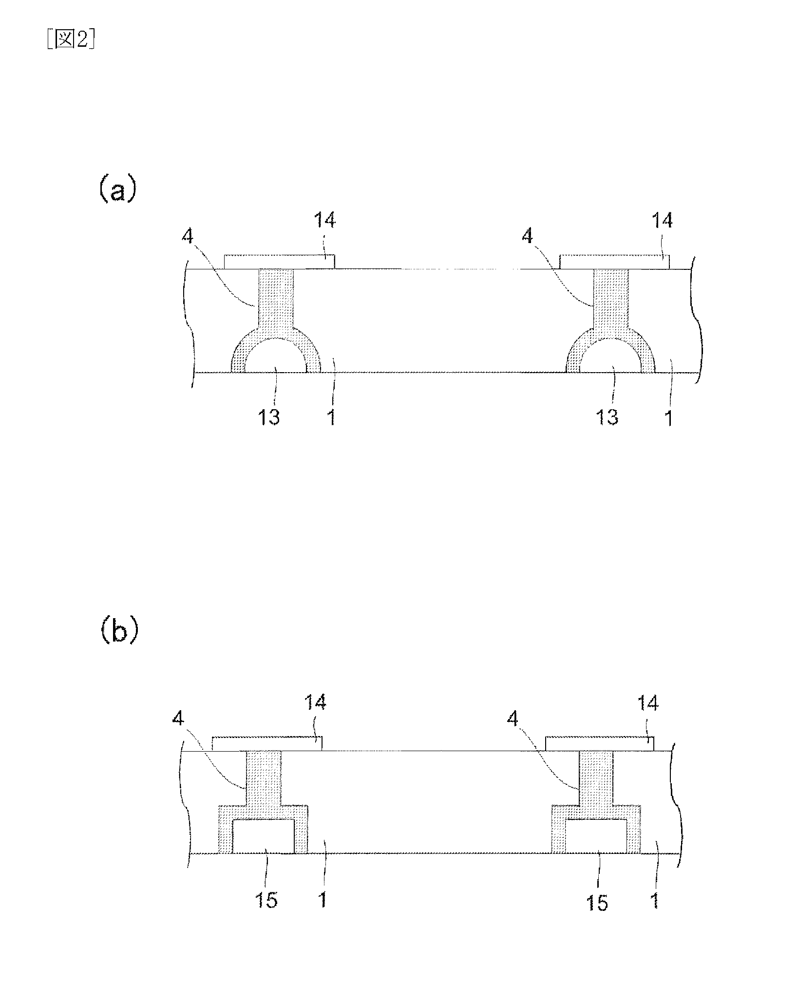
[0082] A method for forming a through electrode will be explained first. An image pickup device according to the present invention is characterized by being formed by wafer level CSP. Of wafer level CSP, a through electrode forming step is especially important. To facilitate formation of an electrode extending through a wafer, there has been proposed a method for polishing the back surface and thinning the wafer (e.g., Patent Document 6: WO2004 / 059740). However, since steps are complicated, and handling of a thin wafer in a processing step after polishing is likely to cause the failure of the wafer or introduction of crystal defects, improvement in steps is desired. The present invention proposes a new method for solving the above-described problem without a back polishing step or by performing polishing or etching at the end of a sequence of steps.
[0083] FIGS. 2(a) and 2(b) are each an example of a step sectional view showing a th...
third embodiment
[0102]FIG. 9 is a schematic configuration view showing another embodiment of an image pickup device according to the present invention. The image pickup device has light-receiving portions 2 formed at a surface portion of a wafer 1 of a chip and a microlens 3 formed corresponding to each of the light-receiving portions 2, as in the case of FIG. 1. Through electrodes 4 are appropriately provided all over the periphery of the wafer 1 and used for supply of power to the light-receiving portions 2 and passing and reception of an electrical signal. Compared with FIGS. 1 and 8, the image pickup device has no rib, and the shape of a transparent plate 8 is different. More specifically, the transparent plate 8 includes a recessed portion 24 whose surface hangs over the light-receiving portions 2 and microlenses 3 on an inner surface side, and a void 9 is formed in the recessed portion 24. Note that arrows and dotted lines in FIG. 9 represent positions at which the wafer 1 is cut by a blade a...
PUM
 Abstract
Description
Claims
Application Information