Pixel arrangement optimization method and device, light-transmitting display panel and display panel

A technology of pixel arrangement and display panel, applied in design optimization/simulation, semiconductor devices, electrical components, etc., can solve the problems of screen display, not full screen, front camera can not display the picture, etc., to improve the photosensitive quality, The effect of reducing the diffraction phenomenon

Active Publication Date: 2020-04-21
KUNSHAN GO VISIONOX OPTO ELECTRONICS CO LTD
View PDF3 Cites 22 Cited by
  • Summary
  • Abstract
  • Description
  • Claims
  • Application Information

AI Technical Summary

Problems solved by technology

However, these electronic devices are not truly full-screen, and cannot be displayed in all areas of the entire screen. For example, the corresponding area of ​​​​the front camera cannot display images.

Method used


Image

  • Pixel arrangement optimization method and device, light-transmitting display panel and display panel
  • Pixel arrangement optimization method and device, light-transmitting display panel and display panel
  • Pixel arrangement optimization method and device, light-transmitting display panel and display panel

Examples


Embodiment Construction

[0058] The characteristics and exemplary embodiments of various aspects of the present invention will be described in detail below. In order to make the purpose, technical solutions and advantages of the present invention clearer, the present invention will be further described in detail below in conjunction with the accompanying drawings and specific embodiments. It should be understood that the specific embodiments described here are only configured to explain the present invention, not to limit the present invention. It will be apparent to one skilled in the art that the present invention may be practiced without some of these specific details. The following description of the embodiments is only to provide a better understanding of the present invention by showing examples of the present invention.

[0059] It should be noted that in this article, relational terms such as first and second are only used to distinguish one entity or operation from another entity or operation...


PUM

PropertyMeasurementUnit
diameteraaaaaaaaaa
diameteraaaaaaaaaa
lengthaaaaaaaaaa

Abstract

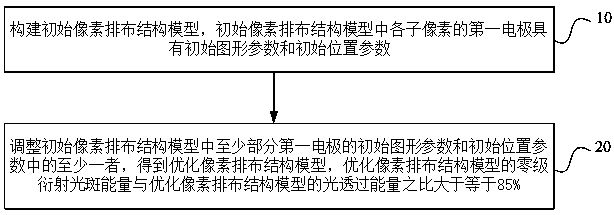
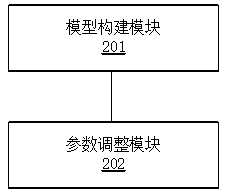
The invention discloses a pixel arrangement optimization method and device, a light-transmitting display panel and a display panel. The method comprises the following steps: constructing an initial pixel arrangement structure model, wherein the first electrode of each sub-pixel in the initial pixel arrangement structure model has an initial pattern parameter and an initial position parameter; adjusting at least one of the initial pattern parameters and the initial position parameters of at least part of the first electrodes in the initial pixel arrangement structure model to obtain an optimized pixel arrangement structure model, and enabling the ratio of the zero-order diffraction light spot energy of the optimized pixel arrangement structure model to the light transmission energy of the optimized pixel arrangement structure model to be greater than or equal to 85%. According to the pixel arrangement optimization method and device and the display panel provided by the embodiment of theinvention, the diffraction phenomenon of the display panel can be displayed.

Description

technical field [0001] The present invention relates to the display field, in particular to a pixel arrangement optimization method, a pixel arrangement optimization device, a light-transmitting display panel and a display panel. Background technique [0002] With the rapid development of electronic devices, users have higher and higher requirements for screen-to-body ratio, so that the full-screen display of electronic devices has attracted more and more attention from the industry. [0003] Traditional electronic devices, such as mobile phones and tablet computers, need to integrate front-facing cameras, earpieces, and infrared sensing elements. In the prior art, a notch or a hole can be made on the display screen, and external light can enter the photosensitive element located below the screen through the notch or hole on the screen. However, none of these electronic devices is a full screen in the true sense, and cannot be displayed in all areas of the entire screen, fo...

Claims


Application Information

Patent Timeline
Patent Type & Authority Applications(China)
IPC IPC(8): G06F30/20H01L27/32H01L51/52
CPCH10K59/353H10K50/813H10K50/822H10K59/352H10K59/121H10K59/80515
Inventor 赵改娜刘如胜邢汝博殷汉权蔡俊飞
Owner KUNSHAN GO VISIONOX OPTO ELECTRONICS CO LTD
Why Eureka
Try Eureka