

PIN diode based on gallium oxide perovskite multilayer stacked structure and preparation method of PIN diode
A PIN diode and multi-layer stacking technology, which is applied in the field of PIN diodes based on Ga2O3/perovskite multi-layer stack structure and its preparation, can solve the problem that photogenerated carriers cannot be separated quickly, the detection performance is not ideal, and the detector To solve problems such as narrow detection band, achieve the effect of simple structure, improved detection performance and low cost
- Summary
- Abstract
- Description
- Claims
- Application Information
AI Technical Summary
Problems solved by technology
Method used
Image



Examples
Embodiment 1
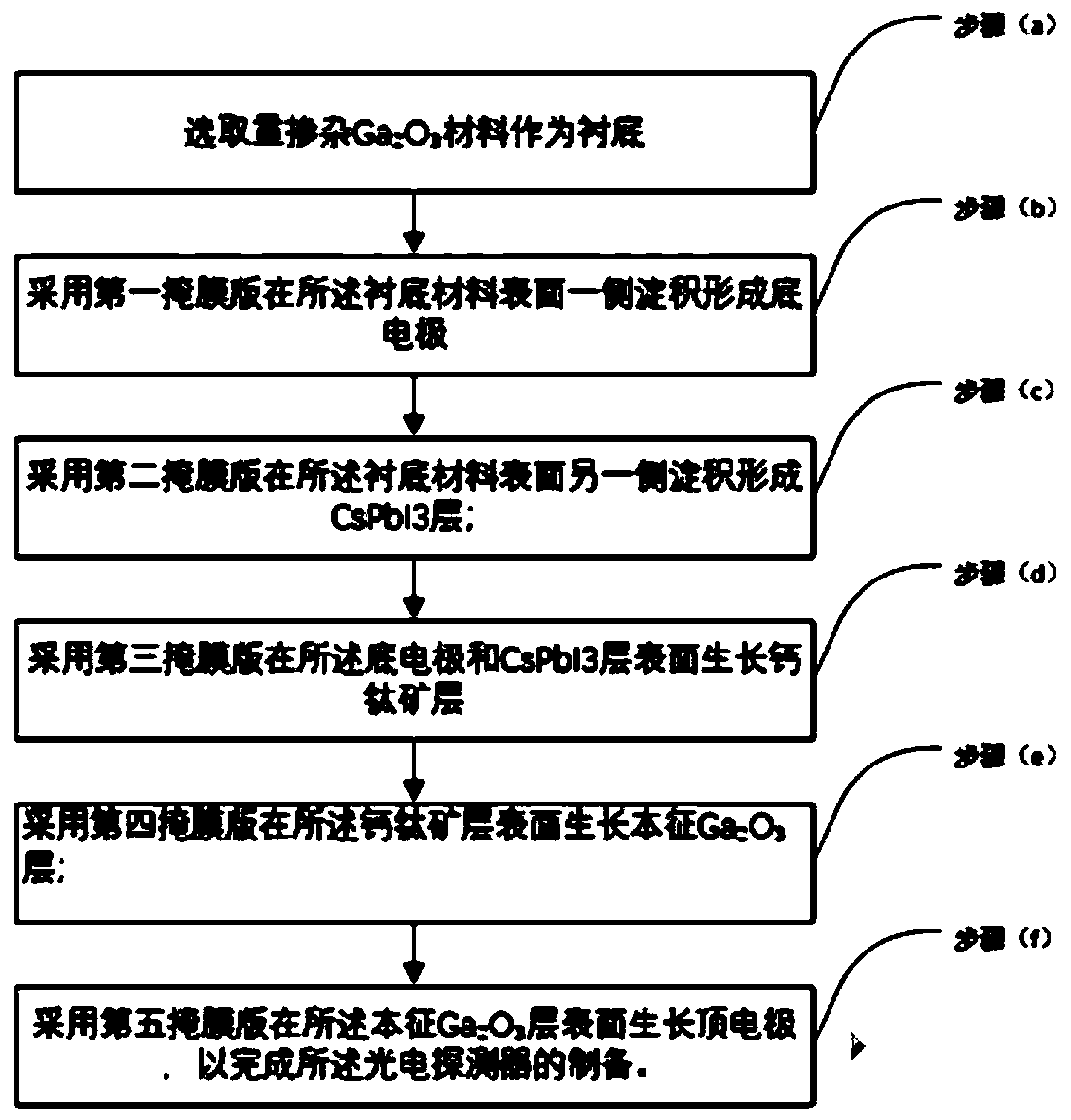
[0044] to combine Figure 1-11 , the present embodiment provides a method for preparing a PIN diode based on gallium oxide perovskite multilayer stacked structure, which specifically includes the following steps:
[0045] (a) Select heavily doped Ga 2 o 3 substrate1;
[0046] (b) in Ga 2 o 3 Bottom electrode 2 is grown on one side of the material surface of substrate 1;
[0047] (c) in Ga 2 o 3 The other side of the substrate 1 material surface grows to form CsPbI 3Layer 3;
[0048] (d) in CsPbI 3 Perovskite layer 4 is grown on the surface of layer 3;
[0049] (e) Growth of intrinsic Ga on the surface of perovskite layer 4 by spin coating method 2 o 3 layer 5;
[0050] (f) In intrinsic Ga 2 o 3 The top electrode is grown on the surface of layer 5, that is, the preparation of the PIN diode is completed.
[0051] Beneficial effects of this embodiment: by selecting heavily doped Ga 2 o 3 As a substrate, intrinsic Ga was grown on the surface of the perovskite lay...
Embodiment 2
[0053] On the basis of Example 1, combined with figure 1 , Figure 6 , step (a) specifically includes the following steps:
[0054] (a1) Choose a thickness of 300-600 μm and a doping concentration of 10 17 -10 18 cm -3 Ga 2 o 3 Substrate sheet 1;
[0055] (a2) Utilize the RCA standard cleaning process to clean the above-mentioned heavily doped Ga 2 o 3 The substrate sheet is cleaned.
[0056] Beneficial effects of this embodiment: through the Ga 2 o 3 The limitation of the thickness and doping concentration of the substrate sheet can improve the electrical performance and mechanical support strength of the substrate sheet.
Embodiment 3
[0058] On the basis of Example 1, combined with figure 1 , Figure 7 , Figure 12 , step (b) specifically includes the following steps:
[0059] (b1) Using the first mask, using the magnetron sputtering process, the Ga 2 o 3 On the surface of the substrate 1, the sputtering power is 40-100W, and the vacuum degree is 4-10×10 -6 Under the condition of Pa, the first metal material with a thickness of 50-200nm is sputtered, and the sputtering ion is selected as Ar. The first metal material here can be selected from ITO, gold, silver, nickel, titanium, platinum, palladium, and FTO materials. Any one of it or one of its alloys; in this embodiment, the sputtering power is selected to be 40W, and the vacuum degree is selected to be 10×10 -6 Pa, the sputtering thickness is 50nm, and the first metal material is ITO.
[0060] (b2) Under the atmosphere of nitrogen and argon, the Ga 2 o 3 The polished surface of the substrate is in contact with the first metal material to form an o...
PUM
| Property | Measurement | Unit |
|---|---|---|
| thickness | aaaaa | aaaaa |
| thickness | aaaaa | aaaaa |
Abstract
Description
Claims
Application Information