

Electrochromic display panel and electronic paper
An electrochromic, display panel technology, applied in nonlinear optics, instruments, optics, etc., can solve the problems of affecting dielectric strength, corrosion reaction, inconvenience for users, etc., to enhance the conductive effect and response speed, electric field. The effect of uniform distribution and production cost saving
- Summary
- Abstract
- Description
- Claims
- Application Information
AI Technical Summary
Problems solved by technology
Method used
Image

Examples
Embodiment 1
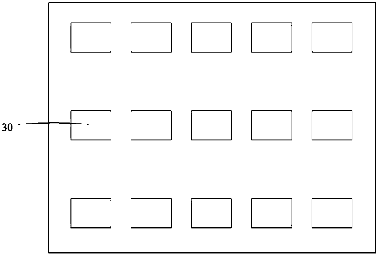
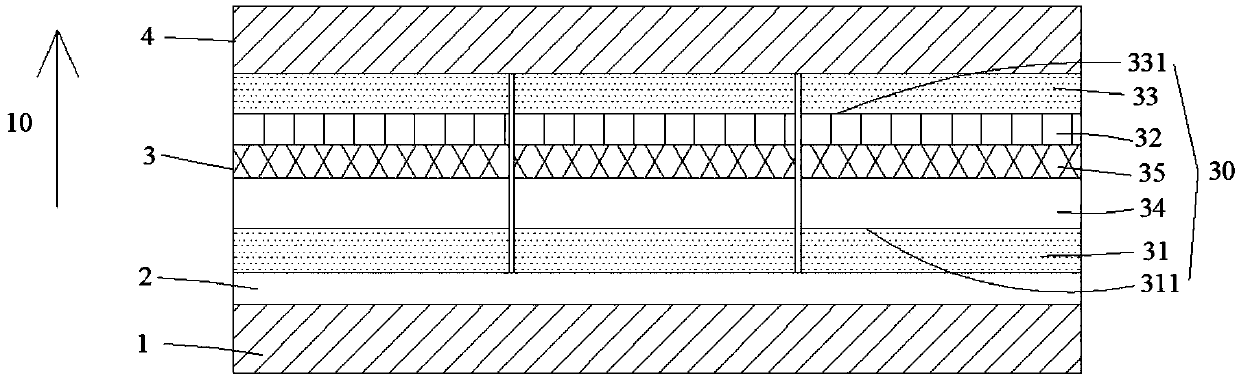
[0047] See Figure 6 The electrochromic display panel shown in this embodiment includes a first substrate 1-1, an electrochromic pixel array 1-2 and a second substrate 1-3 arranged sequentially from bottom to top, and the electrochromic pixel array layer 1- 2 includes a number of electrochromic units 1-20 arranged in an array and independently controlled. The electrochromic unit 1-20 includes a first transparent electrode 1-21, an ion storage layer 1-22, a conductive layer 1-23, black electrochromic pixel layer 1-24, and second transparent electrode 1-25. Wherein, the first transparent electrode 1-21 has a first opposite surface 1-211 opposite to the second transparent electrode 1-25, and the second transparent electrode 1-25 has a second opposite surface opposite to the first transparent electrode 1-21. 1-251, in order to make the electric field distribution between the first transparent electrode 1-21 and the second transparent electrode 1-25 more uniform, this embodiment i...
Embodiment 2
[0050] See Figure 7 The electrochromic display panel shown in this embodiment includes a first substrate 2-1, an electrochromic pixel array 2-2 and a second substrate 2-3 arranged sequentially from bottom to top, and the electrochromic pixel array layer 2- 2 includes a number of electrochromic units 2-20 arranged in an array and independently controlled. The electrochromic unit 2-20 includes a first transparent electrode 2-21, an ion storage layer 2-22, a conductive layer 2-23, black electrochromic pixel layer 2-24, and second transparent electrode 2-25. Wherein, the first transparent electrode 2-21 has a first opposite surface 2-211 opposite to the second transparent electrode 2-25, and the second transparent electrode 2-25 has a second opposite surface opposite to the first transparent electrode 2-21. 2-251, in order to make the electric field distribution between the first transparent electrode 2-21 and the second transparent electrode 2-25 more uniform, this embodiment i...
Embodiment 3
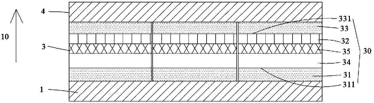
[0053] See Figure 8 , the structure of the electrochromic display panel of this embodiment is basically the same as that of Embodiment 1, and the difference is that in this embodiment, a white reflector is provided between the first substrate 3-1 and the electrochromic pixel array 3-2. Layer 3-5 and adhesive layer 3-51. In this embodiment, the white reflective layer 3-5 is composed of phenolic resin and dispersed titanium oxide, and is provided on the first substrate 3-1 by spin coating. In addition, the thickness of the white reflective layer 3-5 was 20 μm, and the thickness of the adhesive layer 3-51 was 15 μm. Compared with using a viscous white reflective layer to adhere the electrochromic pixel array 3-2, by setting the adhesive layer 3-51, a better adhesion effect can be achieved, so that the electrochromic pixel array 3-2 is more transparent. Stably fixed on the white reflective layer 3-5.
[0054] To sum up: the electrochromic display panel and the electronic paper ...
PUM
| Property | Measurement | Unit |
|---|---|---|
| Thickness | aaaaa | aaaaa |
| Thickness | aaaaa | aaaaa |
Abstract
Description
Claims
Application Information