A Bandpass Filter Based on Sector Microstrip Resonator
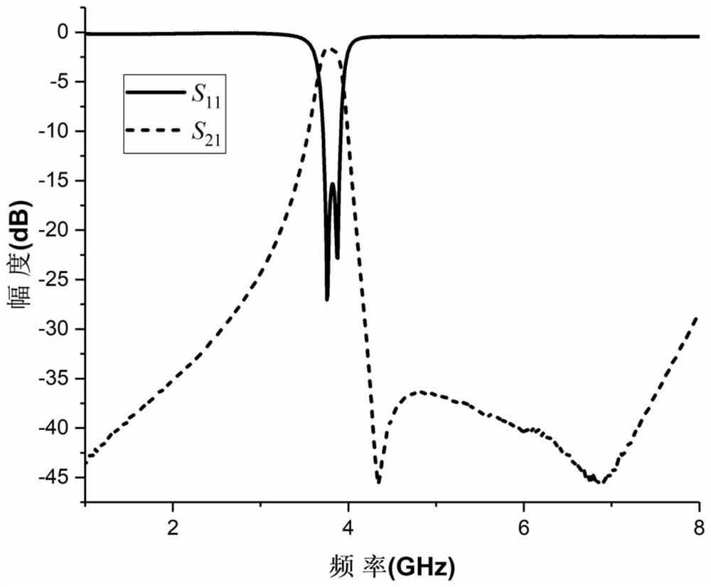
A technology of band-pass filter and microstrip resonance, which is applied in the direction of waveguide devices, circuits, electrical components, etc., can solve the problem of large insertion loss of filters, achieve high stop-band suppression characteristics, and improve the effect of stop-band characteristics
- Summary
- Abstract
- Description
- Claims
- Application Information
AI Technical Summary
Problems solved by technology
Method used
Image
Examples
Embodiment 1
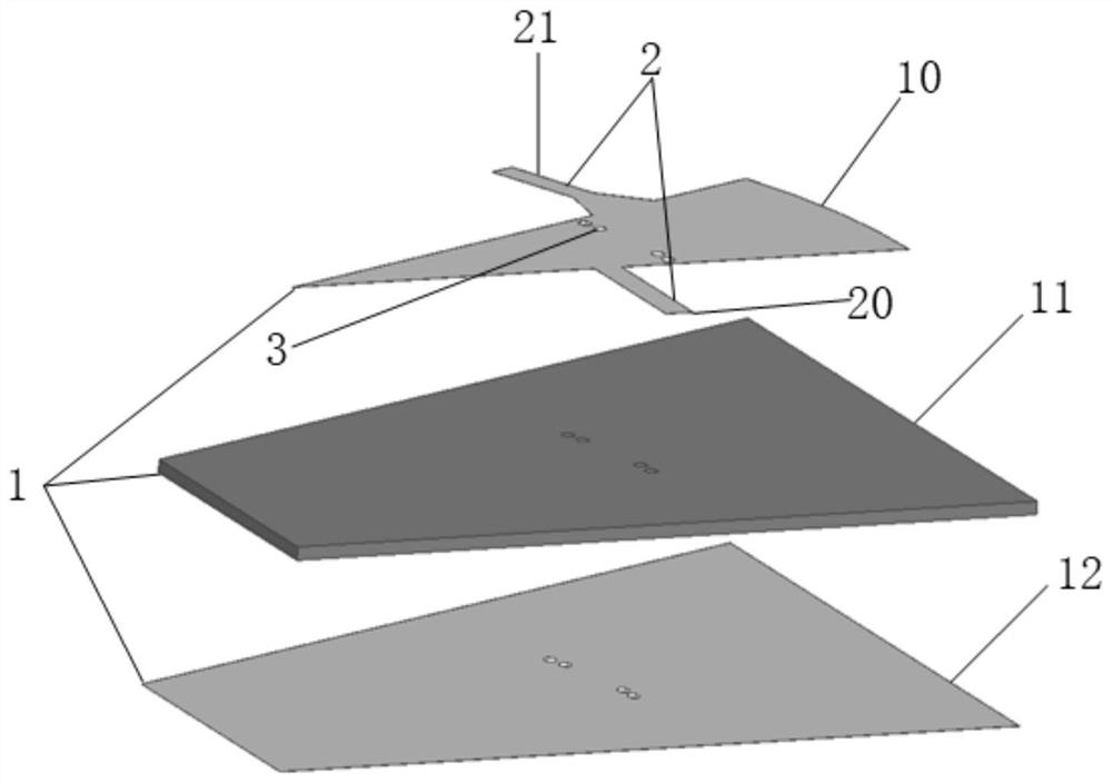
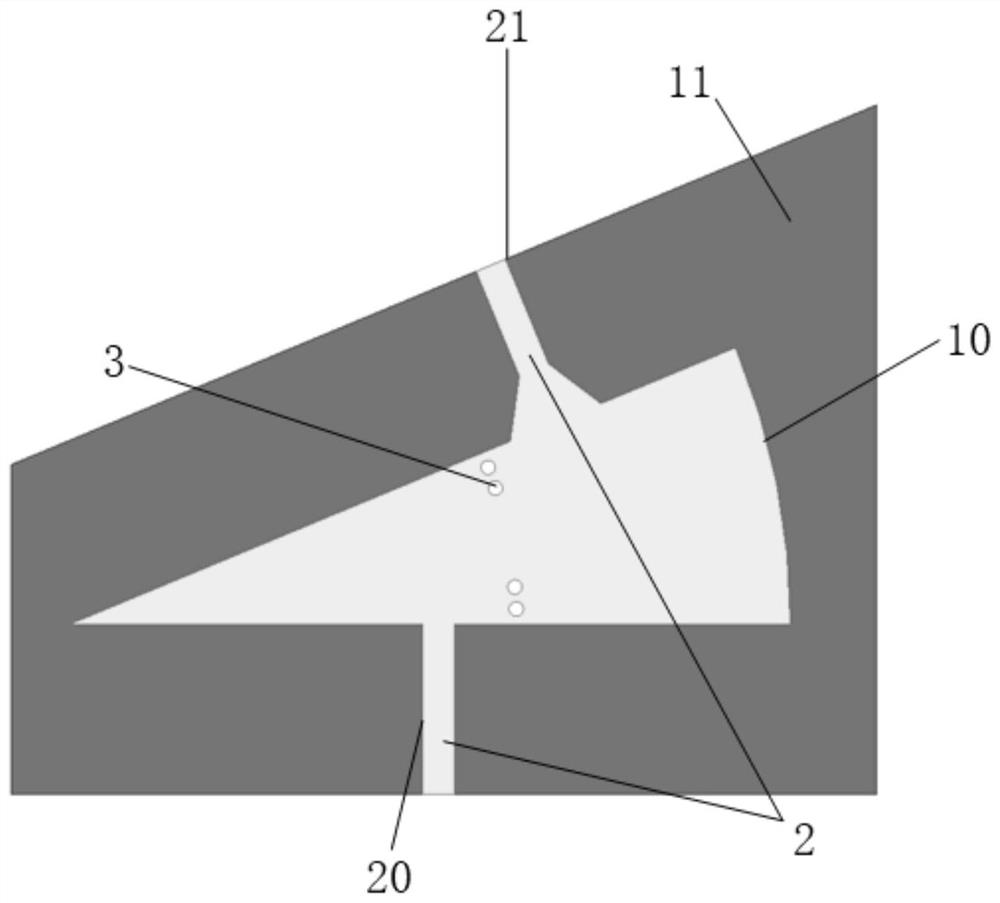
[0020] figure 1 It is a schematic diagram of the overall structure of a specific embodiment of the present invention, including a fan-shaped microstrip resonator 1 , input and output feeders 2 and metallized through holes 3 . The fan-shaped microstrip resonator 1 is sequentially formed by stacking the top fan-shaped metal patch 10, the single-layer dielectric substrate 11 of the middle layer and the bottom metal patch 12 from top to bottom. The radius of the top fan-shaped metal patch 10 It is 27mm, the radian is 22.5°, the thickness is 0.017mm, and the size is equivalent to one sixteenth of the circular metal patch with the same radius. The single-layer dielectric substrate 11 of the middle layer is a low-loss TaconicRF-35 with a thickness of 0.508 mm. It is in the shape of a right-angled trapezoid, with an upper base length of 11.46 mm, a lower base length of 23.92 mm, and a height of 30.1 mm. The size of the bottom metal patch 12 is the same as that of the single-layer die...
Embodiment 2
[0024]In this embodiment, the shapes of the single-layer dielectric substrate 11 and the bottom metal patch 12 of the middle layer are changed from a right-angled trapezoid to any other shape at the same time, while ensuring the shape of the single-layer dielectric substrate 11 of the middle layer and the bottom metal patch 12 The same size and its outer frame size needs to exceed the outer frame size of the fan-shaped metal patch 10 on the top layer plus the input and output feeder 2, and the input and output feeder ports need to be in the outer outline of the single-layer dielectric substrate 11 and the bottom metal patch 12 in the middle layer Online, other parts are completely the same as those in Embodiment 1, and the functions of the present invention can still be realized.
Embodiment 3
[0026] In this embodiment, the transmission line structure of the input and output feeder 2 is changed from a gradual transmission line to a step impedance transmission line structure, and other parts are completely the same as in the first embodiment, and the functions of the present invention can still be realized.
PUM
 Abstract
Description
Claims
Application Information


