Impedance optimization method for circuit board via hole and circuit board

An optimization method and circuit board technology, applied in printed circuit, printed circuit manufacturing, computer design circuit, etc., can solve problems such as high process cost, inability to completely remove via stubs, and affect transmission signal integrity, etc., to achieve optimal impedance , Optimize the effect of impedance continuity

Active Publication Date: 2021-10-22
INSPUR SUZHOU INTELLIGENT TECH CO LTD
View PDF3 Cites 0 Cited by
  • Summary
  • Abstract
  • Description
  • Claims
  • Application Information

AI Technical Summary

Problems solved by technology

However, the back-drilling process cannot completely remove the stumps of the vias, and there are still stumps within about 12mil, which affect the integrity of the transmission signal; although the deep micro-hole technology can completely remove the stumps of the vias, the process cost is relatively high

Method used


Image

  • Impedance optimization method for circuit board via hole and circuit board
  • Impedance optimization method for circuit board via hole and circuit board
  • Impedance optimization method for circuit board via hole and circuit board

Examples


Embodiment Construction

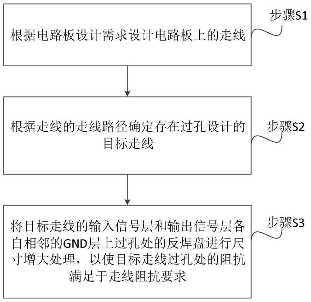
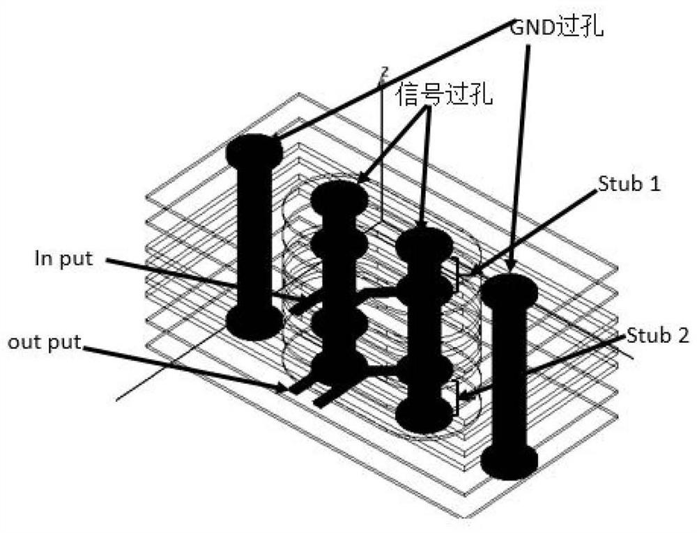
[0037] The core of the present invention is to provide a circuit board via impedance optimization method and a circuit board, by changing the shape of the anti-pad at the via hole to optimize the impedance continuity at the via hole, so as not to increase the process cost To meet the integrity requirements of the transmission signal; moreover, what this application changes is the shape of the anti-pad at the via hole on the adjacent GND layer of the input signal layer and the output signal layer of the wiring, while optimizing the impedance at the via hole Does not affect the impedance of the trace.

[0038] In order to make the purpose, technical solutions and advantages of the embodiments of the present invention clearer, the technical solutions in the embodiments of the present invention will be clearly and completely described below in conjunction with the drawings in the embodiments of the present invention. Obviously, the described embodiments It is a part of embodiments...


PUM


Abstract

The invention discloses a method for optimizing the impedance of a circuit board via hole. The routing on the circuit board is designed according to the design requirements of the circuit board; the target routing of the via hole design exists according to the routing path of the routing; the target routing of the target routing is The size of the anti-pads at the via holes on the adjacent GND layers of the input signal layer and the output signal layer are enlarged so that the impedance of the target trace via holes meets the trace impedance requirements. It can be seen that this application optimizes the impedance continuity at the via hole by changing the shape of the anti-pad at the via hole, so as to meet the integrity requirements of the transmission signal without increasing the process cost; moreover, what this application changes is The shape of the anti-pad at the via hole on the adjacent GND layer of the input signal layer and the output signal layer of the trace will not affect the impedance of the trace while optimizing the impedance of the via hole. The invention also discloses a circuit board, which has the same beneficial effects as the above impedance optimization method.

Description

technical field [0001] The invention relates to the field of circuit board design, in particular to a method for optimizing the impedance of circuit board via holes and a circuit board. Background technique [0002] According to transmission line theory, points of impedance discontinuity affect the integrity of the transmitted signal. However, in the design of circuit board traces, stubs exist at the via holes of the traces, causing the impedance at the via holes to be capacitive, that is, the impedance at the via holes is low, resulting in discontinuous impedance at the via holes, which restricts transmission Signal integrity, especially for traces with high signal transmission rates, the impact of continuity of via impedance is more prominent. In the prior art, back-drilling or deep micro-hole technology is usually used to remove via stubs and optimize impedance at vias. However, the back-drilling process cannot completely remove the stumps of the vias, and there are sti...

Claims


Application Information

Patent Timeline
Patent Type & Authority Patents(China)
IPC IPC(8): H05K3/42H05K3/00
CPCH05K3/0005H05K3/42
Inventor 田民政
Owner INSPUR SUZHOU INTELLIGENT TECH CO LTD
Why Eureka
Try Eureka