A kind of semiconductor structure and its manufacturing method

A manufacturing method and semiconductor technology, applied in the direction of semiconductor devices, electrical components, circuits, etc., can solve the problems of low hole concentration and poor vertical conductivity, and achieve the effect of increasing hole concentration and vertical conductivity

Active Publication Date: 2021-03-05
GUANGDONG INST OF SEMICON IND TECH
View PDF4 Cites 0 Cited by
  • Summary
  • Abstract
  • Description
  • Claims
  • Application Information

AI Technical Summary

Problems solved by technology

[0005] The purpose of this application is to provide a semiconductor structure to solve the problems of low hole concentration and poor vertical conductivity of the p-type AlGaN semiconductor structure in the prior art
[0006] Another object of the present application is to provide a semiconductor structure manufacturing method to solve the problems of low hole concentration and poor vertical conductivity of the p-type AlGaN semiconductor structure in the prior art

Method used


Image

  • A kind of semiconductor structure and its manufacturing method
  • A kind of semiconductor structure and its manufacturing method
  • A kind of semiconductor structure and its manufacturing method

Examples


Embodiment Construction

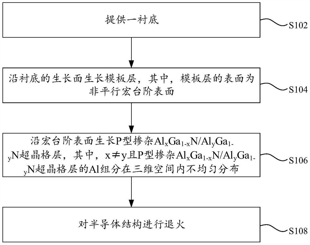
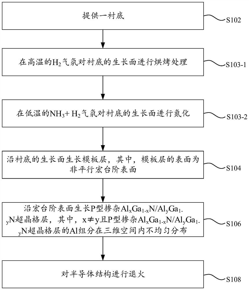
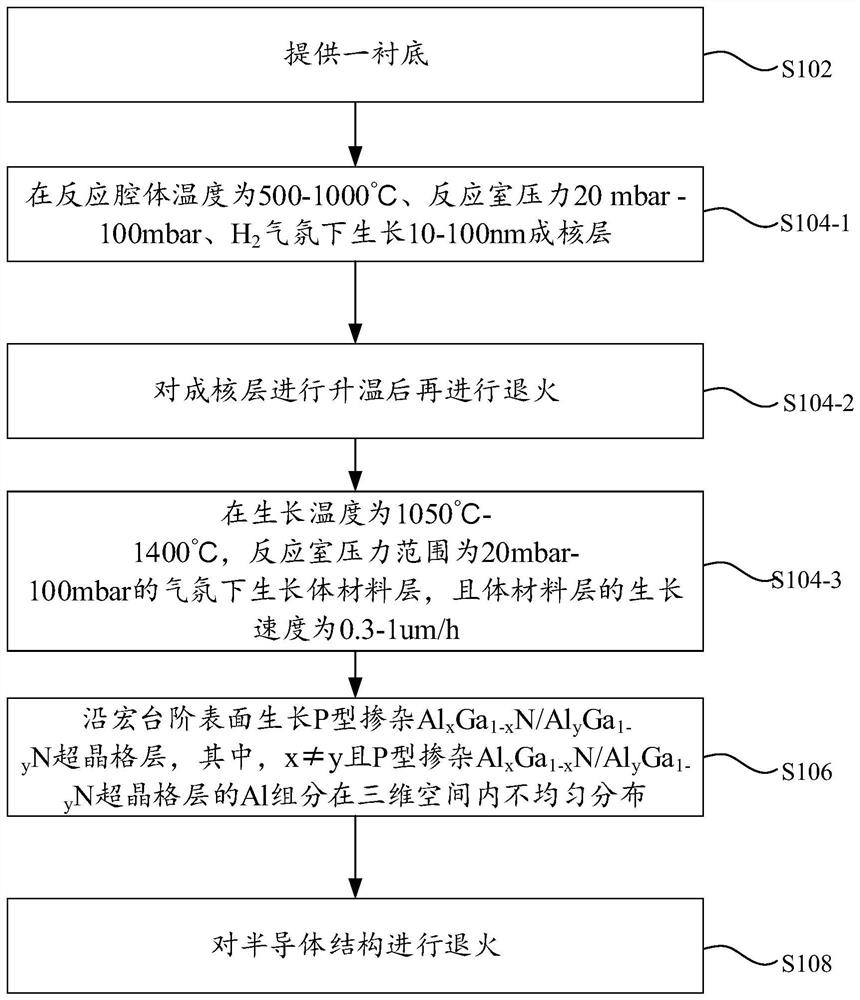
[0046] In order to make the objects, technical solutions, and advantages of the present application, the technical solutions in the present application embodiment will be clearly described, and the described embodiments will be described in conjunction with the drawings in the present application embodiment. It is an embodiment of the present application, not all of the embodiments. Components of the present application embodiments described and illustrated in the drawings herein can be arranged and designed in a variety of different configurations.

[0047] Thus, the detailed description of the embodiments of the present application provided in the drawings is not intended to limit the scope of the present application claimed, but only the selected embodiments of the present application. Based on the embodiments in this application, all other embodiments obtained by those of ordinary skill in the art without creative labor, are the scope of the present application.

[0048] It sh...


PUM

PropertyMeasurementUnit
thicknessaaaaaaaaaa
heightaaaaaaaaaa
surface roughnessaaaaaaaaaa

Abstract

The invention provides a semiconductor structure and a manufacturing method thereof, and relates to the technical field of semiconductor material preparation. The semiconductor structure comprises a substrate, a template layer which is connected with the growth surface of the substrate, wherein the surface of the template layer is a non-parallel macro step surface, and a P-type doped Al < x > Ga <1-x > N / Al < y > Ga < 1-y > N superlattice layer which is connected with the macro step surface, x is not equal to y, and Al components of the P-type doped Al < x > Ga < 1-x > N / Al < y > Ga < 1-y > Nsuperlattice layer are unevenly distributed in three-dimensional space. The semiconductor structure and the manufacturing method thereof provided by the invention have the effects of improving the hole concentration of the material and improving the longitudinal conductivity of the semiconductor structure.

Description

Technical field [0001] The present application relates to the preparation of semiconductor materials, and in particular, there is a semiconductor structure and a method of fabricating it. Background technique [0002] AlgaN-based DUV-LED (deep UV LED) is the only deep UV solid state light source that can replace mercury lamps, which has good portability, full solid, low energy, long life than traditional mercury lamps. Pollution, many advantages, the market prospects are extremely broad. At present, the latex light of deep UV LED is relatively low, and one of the most important reasons is to low the hole concentration of P-type AlGaN. [0003] The low-air concentration of P-type AlGaN extension not only seriously affects the injection of holes, which greatly reduces the radiation composite efficiency of quantum wells. At the same time, it will greatly improve the overall resistance of the device, resulting in a rapid deterioration of high junction temperature and the life of the ...

Claims


Application Information

Patent Timeline
Patent Type & Authority Patents(China)
IPC IPC(8): H01L33/06H01L33/24H01L33/32H01L33/00
CPCH01L33/007H01L33/06H01L33/24H01L33/325
Inventor 张康赵维贺龙飞何晨光吴华龙李成果刘云洲陈志涛
Owner GUANGDONG INST OF SEMICON IND TECH
Why Eureka
Try Eureka