
An ultra-high time-resolved in-situ 5d TEM test device and its application method
A time-resolved, testing device technology, applied in measurement devices, material analysis using radiation, material analysis using wave/particle radiation, etc., can solve the problem of limited control range, inability to accurately locate samples, lack of microstructure testing devices and methods and other issues to achieve the effect of a wide range of applications
- Summary
- Abstract
- Description
- Claims
- Application Information
AI Technical Summary
Problems solved by technology
Method used
Image

Examples
Embodiment 1
[0060] Obtain PbS through centrifugation and other pretreatments and make a PbS sample cell. The sample cell includes a thin-layer solution containing PbS nanoparticle pairs, and two identical Si 3 N 4 Disc (diameter 800nm, thickness 20nm), symmetrically wrapped in Si 3 N 4 Two identical Si wafers (diameter 800nm, thickness 200nm) of the wafer, Si 3 N 4 There is a square through hole of 300nm×300nm in the middle of the wafer, and a corresponding square groove of 300nm×300nm in the middle of the Si wafer. The thin layer solution is sealed in the space of the through hole and the groove, and the whole is bonded by epoxy Agent packaging to ensure airtightness and vacuum.
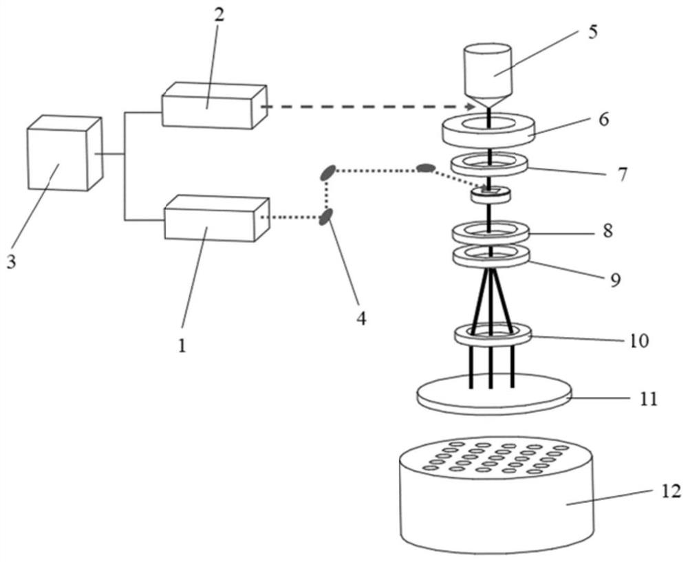
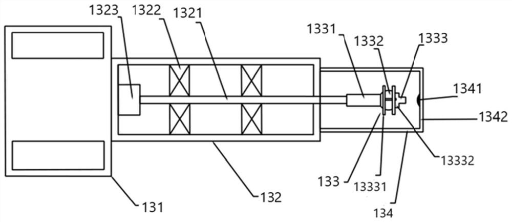
[0061]After loading the PbS sample cell into the sample grid, install it on the sample chuck 13332 of the rod head 133, move the Ag sample and make it slowly approach the non-diamond-containing area 1342 of the metal pressure ring 134, and when it touches the metal pressure ring After the non-diamond-conta...
Embodiment 2
[0064] The Ag sample is obtained through pretreatment such as abrasion reduction and an Ag sample rod is made, and the Ag sample rod is loaded into the sample grid and installed on the sample chuck 13332 of the rod head 133 .
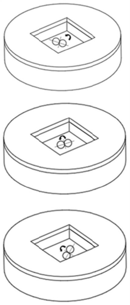
[0065] Move the Ag sample rod through the in-situ operation module and make it slowly approach the diamond-containing region 1341 of the metal pressure ring 134 , and continue to compress after touching the diamond-containing region 1341 of the metal pressure ring 134 and gradually begin to produce microscopic deformation. Wherein, mainly including the diamond-containing region 1341 not contacting the metal pressure ring 134, the diamond-containing region 1341 contacting the metal pressure ring 134 and the diamond-containing region 1341 pressing the metal pressure ring 134 are totally 3 states, such as Figure 4 shown.
[0066] At this time, through the imaging module and the observation and recording module, the changes in the internal organization and...
PUM
| Property | Measurement | Unit |
|---|---|---|
| diameter | aaaaa | aaaaa |
| thickness | aaaaa | aaaaa |
Abstract
Description
Claims
Application Information