Finterprint identification device and electronic device
A fingerprint identification and fingerprint image technology, which is applied in character and pattern recognition, acquisition/organization of fingerprints/palmprints, detection of live finger shapes, etc., can solve problems such as hidden dangers of fingerprint application security
- Summary
- Abstract
- Description
- Claims
- Application Information
AI Technical Summary
Problems solved by technology
Method used
Image
Examples
Embodiment 1
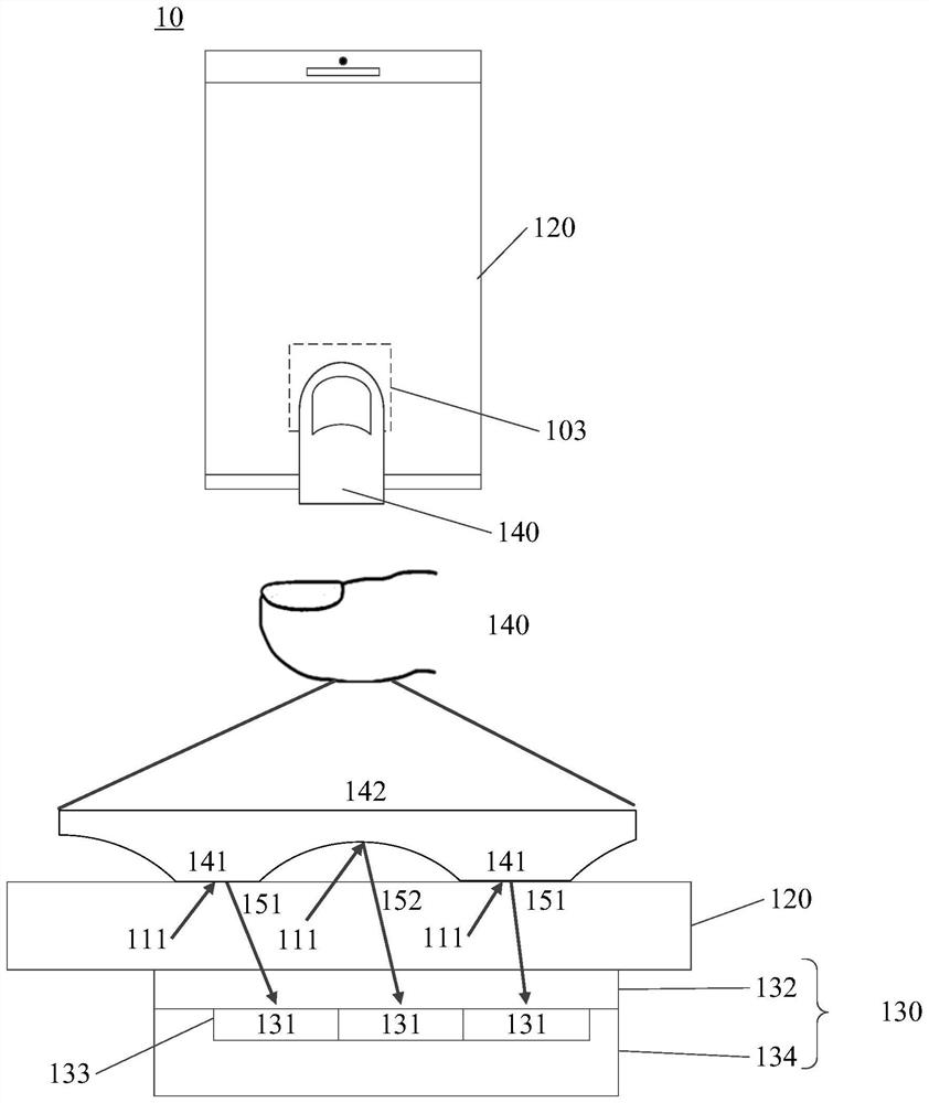
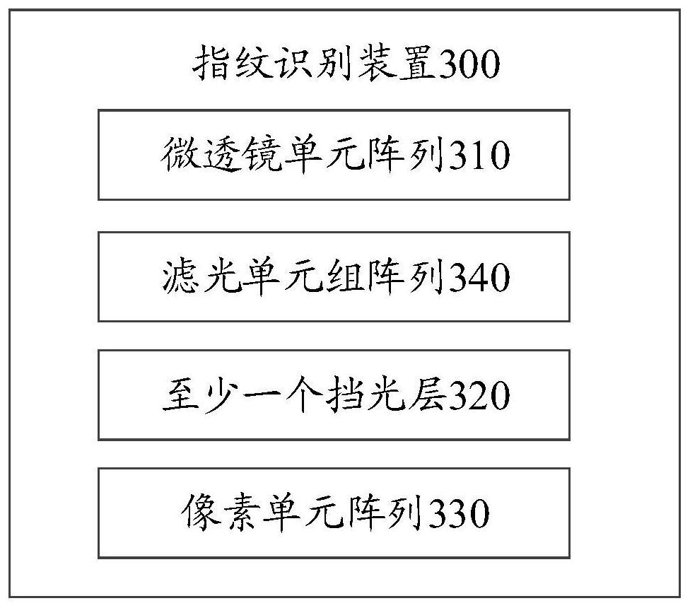
[0097] In this Example 1, as Figure 4 and Figure 5 As shown, the fingerprint recognition device may include a microlens unit array 310 , at least one light blocking layer 320 , a pixel unit array 330 and a filter unit array 340 .
[0098] Wherein, each microlens unit group in the microlens unit array 310 includes 4 microlens units, each microlens unit includes a microlens 311, and each microlens in the four microlens units is used for The optical signals in the four directions are transmitted to the corresponding pixel units, and the filter unit corresponding to each microlens unit is located on the optical path in the first direction, that is, the filter unit corresponding to each microlens unit is used for For the optical signal of a specific wavelength band among the optical signals transmitted in the first direction, the specific wavelength band is a wavelength band that can be transmitted by the filter unit.
[0099] As an example, each microlens is disposed directly ab...
Embodiment 2
[0120] Optionally, as in Figure 7 As shown, the microlens unit group is an array composed of 2*2 microlens units, each microlens unit includes 2*2 microlenses, and each filter unit group includes sixteen filter units, each filter The light unit corresponds to a microlens and a pixel unit. That is, the four microlenses in each microlens unit correspond to four filter units of the same color, for example, Figure 7 The 2*2 microlenses in the upper left corner of the center are a microlens unit, and the corresponding filter units are 4 filter units of the same color, for example, a red light filter unit; and for example, Figure 7 The 2*2 microlenses in the lower right corner are a microlens unit, and the corresponding filter units are 4 filter units of the same color, for example, a blue light filter unit.
[0121] It should be noted that the difference between this embodiment 2 and embodiment 1 is that one microlens unit corresponds to the number of filter units of the same ...
Embodiment 3
[0125] like Figure 8 As shown, the fingerprint recognition device may include a microlens unit array 310 , at least one light blocking layer 320 , a pixel unit array 330 and a filter unit array 340 .
[0126] The at least one light-shielding layer 320 includes a bottom light-shielding layer 321 and a top light-shielding layer 322, wherein the bottom light-shielding layer 321 and the top light-shielding layer 322 are respectively provided with each micro lens in the plurality of microlenses. A set of small holes corresponding to a lens.
[0127] The pixel units in the pixel unit array 330 arranged under the microlens are used to receive the light in the four directions converged by the microlens and transmitted through the small holes in the bottom light-blocking layer and the top light-blocking layer. light signal.
[0128] Specifically, the microlens unit array 310 includes an array of 3*3 microlens units, each microlens unit includes a microlens, the pixel unit group is a...
PUM
 Abstract
Description
Claims
Application Information
 - R&D Engineer
- R&D Manager
- IP Professional
- Industry Leading Data Capabilities
- Powerful AI technology
- Patent DNA Extraction
Browse by: Latest US Patents, China's latest patents, Technical Efficacy Thesaurus, Application Domain, Technology Topic, Popular Technical Reports.
© 2024 PatSnap. All rights reserved.Legal|Privacy policy|Modern Slavery Act Transparency Statement|Sitemap|About US| Contact US: help@patsnap.com


