
Display device

A technology for display devices and display layers, applied in optics, instruments, electrical components, etc., can solve problems such as increased production costs, achieve the effects of reducing waste, reducing manufacturing costs and processes, and shortening the manufacturing process

Pending Publication Date: 2020-12-15
SAMSUNG DISPLAY CO LTD
View PDF0 Cites 2 Cited by
  • Summary
  • Abstract
  • Description
  • Claims
  • Application Information

AI Technical Summary

Problems solved by technology

Since the thickness of the polarizing film is as thick as about 200 μm, it is difficult to make the organic light emitting diode display device thin, and its production cost increases

Method used


Image

  • Display device
  • Display device
  • Display device

Examples


Embodiment Construction

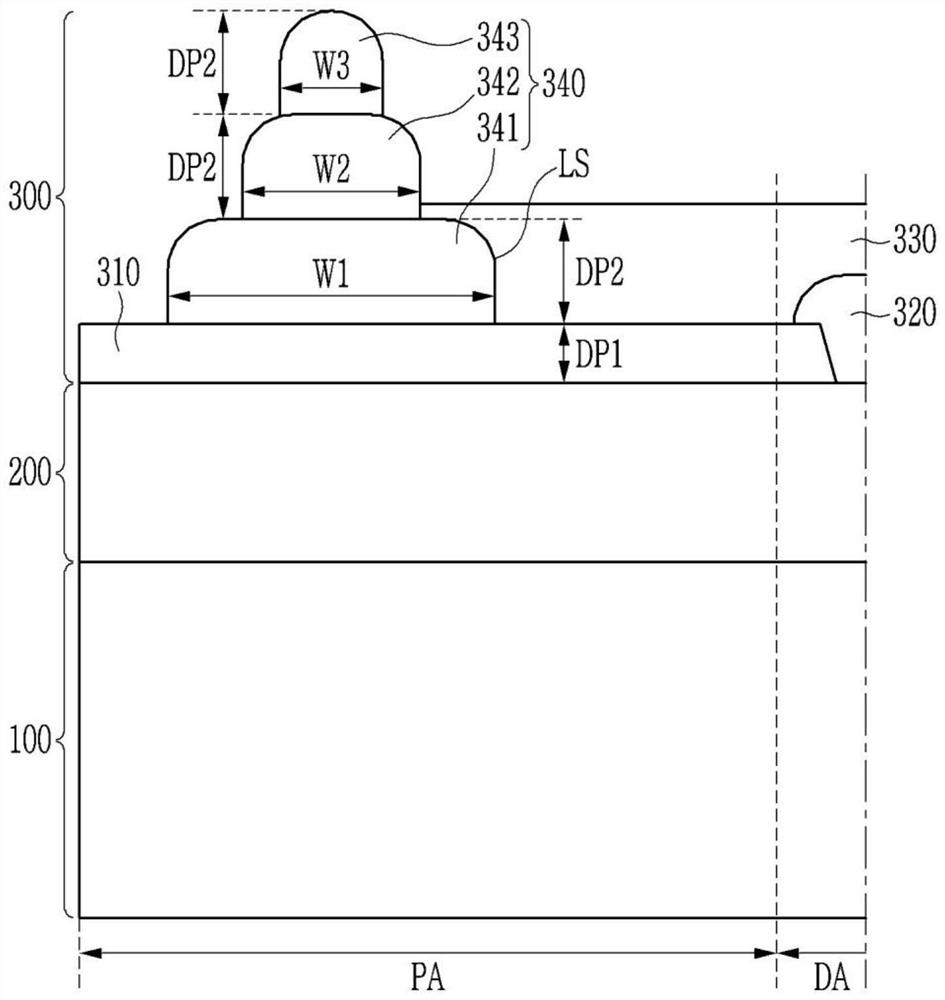
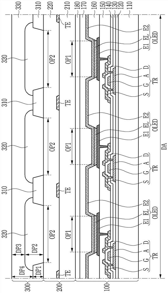
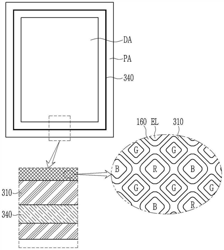
[0053] In the following description, for purposes of explanation, numerous specific details are set forth in order to provide a thorough understanding of various exemplary embodiments or implementations of the present disclosure. As used herein, "embodiment" and "implementation" are interchangeable terms that refer to non-limiting examples of apparatus or methods that employ one or more of the inventive concepts disclosed herein . It is evident, however, that the various exemplary embodiments may be practiced without these specific details, or with one or more equivalent arrangements. In other instances, well-known structures and devices are shown in block diagram form in order to avoid unnecessarily obscuring the various exemplary embodiments. Furthermore, various exemplary embodiments may be different, but are not necessarily exhaustive. For example, the specific shape, configuration, and characteristics of an exemplary embodiment may be used or implemented in another exem...


PUM


Abstract

The invention relates to a display device that includes: a display layer having a display area including a plurality of pixel areas and a peripheral area at least partially surrounding the display area; and a cover layer disposed on the display layer to encapsulate the display area. The cover layer includes: a light blocking portion overlapping the display area and the peripheral area and including a plurality of openings to transmit light from the plurality of pixel areas and to block light in the peripheral area; a first protrusion disposed on the light blocking portion in the peripheral area and surrounding the display area; and an overcoating layer covering the display area and contacting a lateral surface of the first protrusion.

Description

technical field [0001] Exemplary embodiments of the present disclosure relate generally to a display device and a method for manufacturing a display device, and more particularly, to a display device including an encapsulation layer and a photomask process without using a photomask that would damage a light emitting element such as an organic light emitting diode. A method of manufacturing a display device in the case of. Background technique [0002] An organic light emitting diode display device includes two electrodes and a light emitting layer disposed between the two electrodes, and electrons injected from one electrode and holes injected from the other electrode are combined with each other in the light emitting layer to generate excitons. The generated excitons transition from an excited state to a ground state, releasing energy to emit light. [0003] An organic light emitting diode display device includes a plurality of pixels each including an organic light emitti...

Claims


Application Information

Patent Timeline
Patent Type & Authority Applications(China)
IPC IPC(8): H01L27/32
CPCH10K59/353H10K59/38H10K59/40H10K59/8791H10K59/873H10K59/12G02F1/133512H01L33/44H01L27/14678G02F1/133514G02F1/136209H10K50/844H10K71/00
Inventor 李进炯金寿桢孙廷昊李美禾李允浩
Owner SAMSUNG DISPLAY CO LTD
Learn More