

DRAM memory timing configuration method and device
A timing configuration, memory technology, applied in the direction of instrument, input/output to record carrier, calculation, etc., can solve the problems of low bandwidth utilization, unidentifiable memory particle type, etc., to achieve the effect of improving memory efficiency
- Summary
- Abstract
- Description
- Claims
- Application Information
AI Technical Summary
Problems solved by technology
Method used
Image

Examples
Embodiment Construction
[0035] In order to explain in detail the technical content, structural features, achieved goals and effects of the technical solution, the following will be described in detail in conjunction with specific embodiments and accompanying drawings.
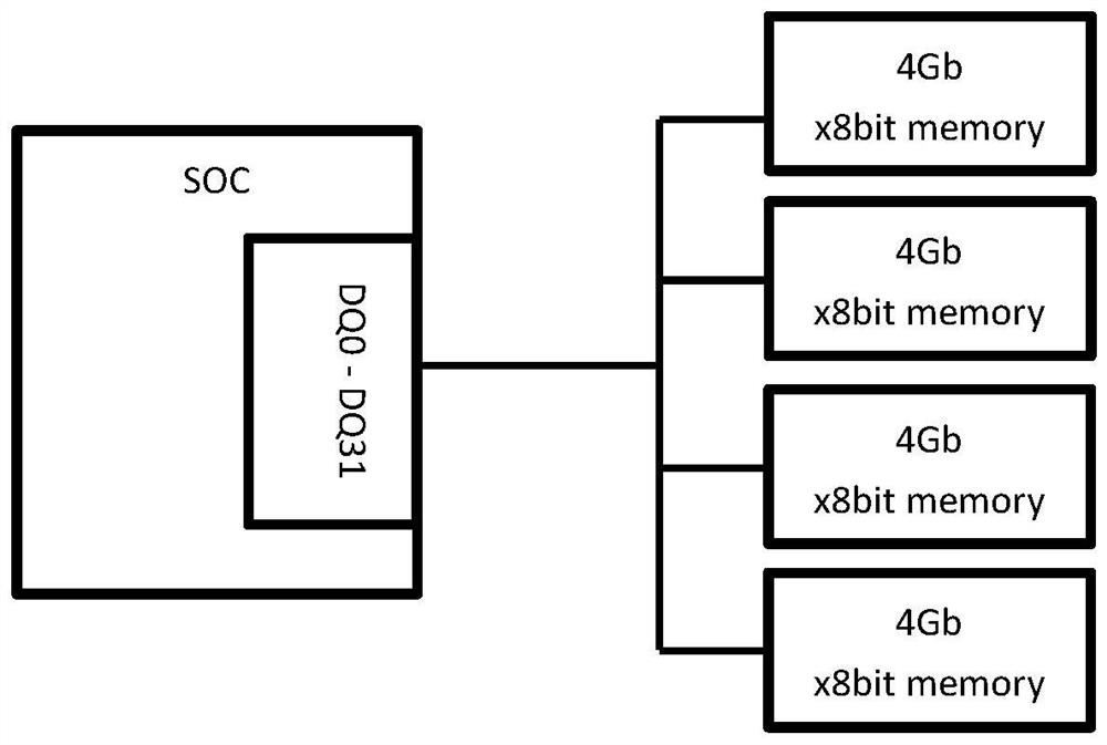
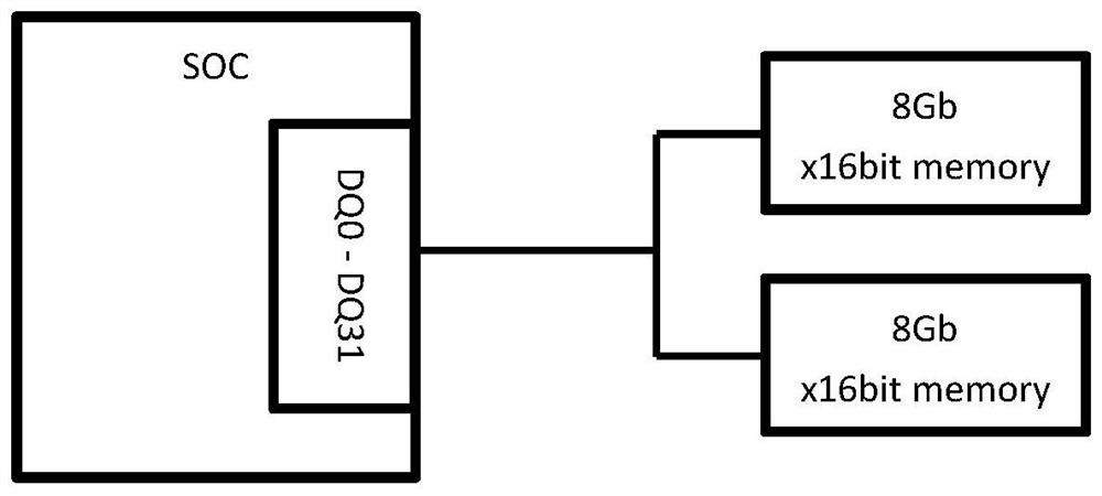
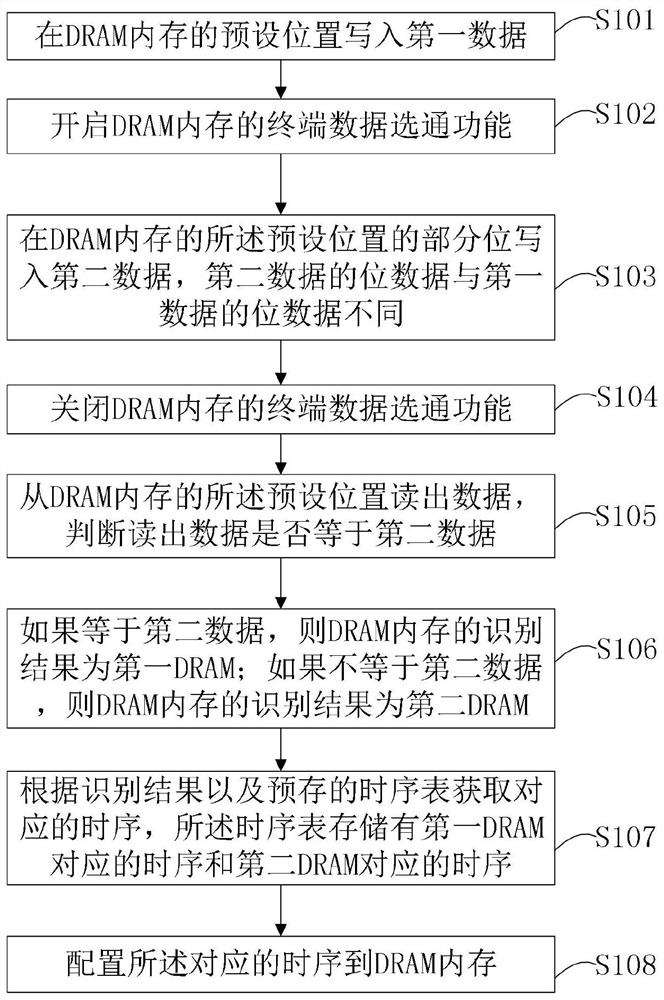
[0036] see Figure 3 to Figure 6 , this embodiment provides a DRAM memory timing configuration method, which is used to configure the DRAM memory as the timing of the first DRAM or as the timing of the second DRAM. The timing here may be timing related to the line width or capacity of DRAM memory particles, such as tRFC (row address refresh cycle) timing. The first DRAM has a first line width, the second DRAM has a second line width, the first line width is different from the second line width, the first DRAM has a terminal data gating function, and the second DRAM No terminal data strobe capability.
[0037] Among them, the terminal data strobe function (TDQS function) is only available in x8bit DDR3 or DDR4, and the corresponding ...
PUM
 Abstract
Description
Claims
Application Information