Supercharge Your Innovation With Domain-Expert AI Agents!

Electronic device with fingerprint sensing function

A technology for electronic devices and sensing circuits, which is applied in the acquisition/organization of fingerprints/palmprints, circuits, electrical components, etc., can solve the problems of increased manufacturing cost, volume or thickness of electronic devices, and reduce the overall device volume or thickness. , the effect of reducing the space of functional modules

Pending Publication Date: 2021-01-01
EGIS TECH
View PDF0 Cites 0 Cited by
  • Summary
  • Abstract
  • Description
  • Claims
  • Application Information

AI Technical Summary

Problems solved by technology

In other words, a general fingerprint sensor will increase the overall device volume or thickness of the electronic device, and further lead to an increase in the manufacturing cost of the electronic device.

Method used


Image

  • Electronic device with fingerprint sensing function
  • Electronic device with fingerprint sensing function
  • Electronic device with fingerprint sensing function

Examples


Embodiment Construction

[0036] Reference will now be made in detail to the exemplary embodiments of the present invention, examples of which are illustrated in the accompanying drawings. Wherever possible, the same reference numbers will be used in the drawings and description to refer to the same or like parts.

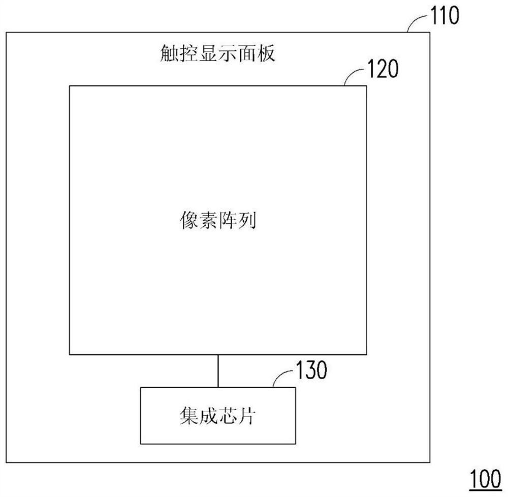
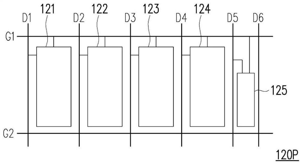
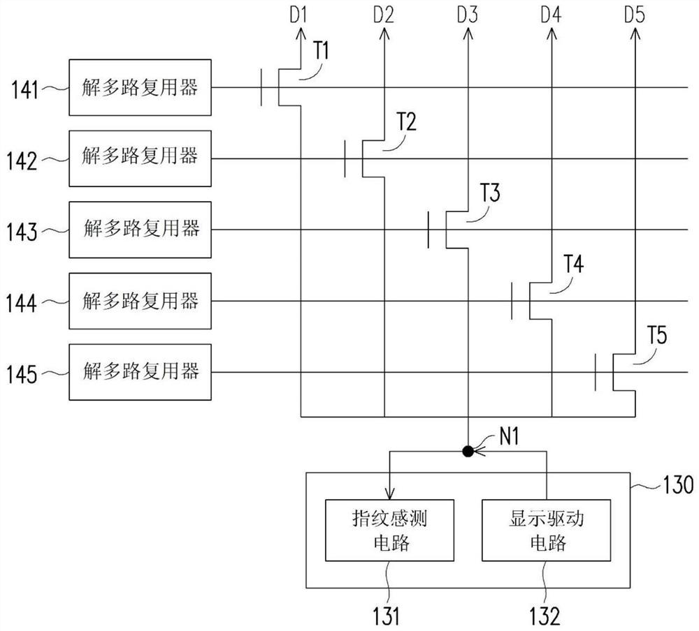
[0037] figure 1 is a schematic diagram of an electronic device according to an embodiment of the present invention. refer to figure 1 , the electronic device 100 includes a touch display panel 110 , a pixel array 120 and an integrated chip (Integrated chip, IC) 130 . The pixel array 120 is electrically connected to the integrated chip 130 . In this embodiment, the touch display panel 110 may, for example, include a glass substrate and a touch panel, wherein the pixel array 120 is formed on the glass substrate in an active area (AA) of the touch display panel 110 . The integrated chip 130 is formed in a peripheral area (Peripheral area, PA) of the touch display panel 110 . In this embod...


PUM


Abstract

The invention provides an electronic device with a fingerprint sensing function. The electronic device comprises a touch display panel and an integrated chip. The touch display panel comprises a pixelarray. The integrated chip is electrically connected to the pixel array. The integrated chip comprises a fingerprint sensing circuit and a display driving circuit. The fingerprint sensing circuit andthe display driving circuit are electrically connected to the plurality of display data lines and the sensing data lines through the same pin. The plurality of display data lines are electrically connected to the plurality of color sub-pixels of the pixel array respectively. The sensing data lines are electrically connected to a plurality of fingerprint sensing pixels of the pixel array. The plurality of color sub-pixels are a plurality of organic light emitting diode pixels.

Description

technical field [0001] The invention relates to a device, in particular to an electronic device with a fingerprint sensing function. Background technique [0002] In recent years, fingerprint identification technology has been widely used in various electronic devices to provide various identity login or identity verification functions. At present, the existing technical principles of fingerprint identification include optical, capacitive, thermal and ultrasonic. In this regard, since the above-mentioned fingerprint sensors are installed in the electronic device, the fingerprint sensor usually needs to occupy a part of the device volume of the electronic device, wherein a general fingerprint sensor can be installed or hung on the bottom of the screen, the Home button or the body of the electronic device, for example. back etc. In other words, the general fingerprint sensor will increase the overall device volume or thickness of the electronic device, and further increase t...

Claims


Application Information

Patent Timeline
IPC IPC(8): G06K9/00G06F3/041H01L27/32
CPCG06F3/0412G06F3/0416G06V40/1306H10K59/40H10K59/65H10K59/12G06F3/0443G09G3/20G09G2300/0426G09G2310/027H10K59/351H10K59/131G06V40/1318G09G3/3275G09G2310/08G06V40/13G09G2310/0264G09G3/2085
Inventor 黄耀立林郁轩彭子洋
Owner EGIS TECH
Features
  • R&D
  • Intellectual Property
  • Life Sciences
  • Materials
  • Tech Scout
  • Unparalleled Data Quality
  • Higher Quality Content
  • 60% Fewer Hallucinations
Learn More