Touch panel defect detection system and touch panel defect detection method
A touch panel and defect detection technology, which is applied in image data processing, instruments, electrical digital data processing, etc., can solve problems affecting the touch effect of the touch panel, and achieve the effect of improving the accuracy of capture and effective defect detection
- Summary
- Abstract
- Description
- Claims
- Application Information
AI Technical Summary
Problems solved by technology
Method used
Image


Examples
no. 1 example
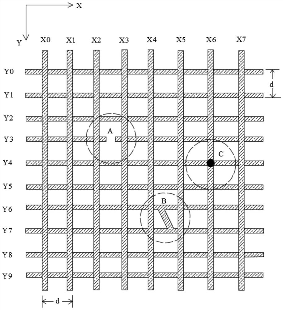
[0078] Please refer to image 3 , image 3 A schematic structural frame diagram of the touch panel defect detection system 10 provided in the first embodiment of the present application is shown.
[0079] The touch panel defect detection system 100 provided in this embodiment may include a touch panel scanning device 110 , a pattern defect locating device 120 , an image scanning device 130 , an image processing device 140 and an image capture device 150 .
[0080] The touch panel scanning device 110 is used for scanning the touch panel to be tested to determine whether the touch pattern of the touch panel to be tested is defective.
[0081] The pattern defect locating device 120 is used for locating the target position area where the defect of the touch pattern is located on the touch panel to be inspected when there is a defect in the touch pattern of the touch panel to be inspected.
[0082] The image scanning device 130 is configured to scan and obtain an image of the tar...
no. 2 example
[0106] Please refer to Figure 8 , the second embodiment of the present application provides a touch panel defect detection system 100 having the same inventive concept as the first embodiment. The image scanning device 130 is not included. The touch panel defect detection system 100 provided by this embodiment will be described in detail below.
[0107] In this embodiment, the touch panel defect detection system 100 may include a touch panel scanning device 110 , a pattern defect locating device 120 , an image processing device 140 and an image capture device 150 .
[0108] The touch panel scanning device 110 is used for scanning the touch panel to be tested to determine whether the touch pattern of the touch panel to be tested is defective.
[0109] The pattern defect locating device 120 is used for locating the target position area where the defect of the touch pattern is located on the touch panel to be inspected when there is a defect in the touch pattern of the touch p...
no. 3 example
[0116] This embodiment provides a method for defect detection of a touch panel, please refer to Figure 10 , the defect detection method of the touch panel may include the following steps.
[0117] Step S110 , scanning the touch panel to be tested, and determining whether there is a defect in the touch pattern of the touch panel to be tested according to the scanning result.
[0118] Please refer to the first embodiment for the specific scanning principle, and will not go into details here. When it is determined that the touch pattern of the touch panel to be detected is defective, enter step S120; when it is determined that the touch pattern of the touch panel to be detected does not exist When there is a defect, the defect detection of the touch panel to be detected is ended.
[0119] In this embodiment, this step can be implemented by using the touch panel scanning device 110 in the first embodiment.
[0120] Step S120, locating the target position area where the touch pa...
PUM
 Abstract
Description
Claims
Application Information