Silicon-based organic electroluminescent micro-display and preparation method thereof

A micro-display and luminescent technology, which is applied in the fields of electrical solid-state devices, semiconductor/solid-state device manufacturing, circuits, etc., can solve the problems of sub-pixel lateral leakage, color gamut reduction, cross-color, etc., so as to improve hole injection ability and avoid Mutual cross-color, improve the effect of work function

Pending Publication Date: 2021-03-16
南京昀光科技有限公司
View PDF4 Cites 1 Cited by
  • Summary
  • Abstract
  • Description
  • Claims
  • Application Information

AI Technical Summary

Problems solved by technology

And because the current preparation method of silicon-based organic electroluminescent microdisplay is to use Open mask to vapor-deposit a layer of this p-doped organic material, and because the conductivity of NPD-9 material is extremely strong, the pitch of sub-pixels is very small ( Generally, it is around 1um), so it is easy to cause lateral leakage between sub-pixels, and then cross-color will occur between adjacent sub-pixels, resulting in a decrease in color gamut

Method used


Image

  • Silicon-based organic electroluminescent micro-display and preparation method thereof
  • Silicon-based organic electroluminescent micro-display and preparation method thereof
  • Silicon-based organic electroluminescent micro-display and preparation method thereof

Examples


Embodiment Construction

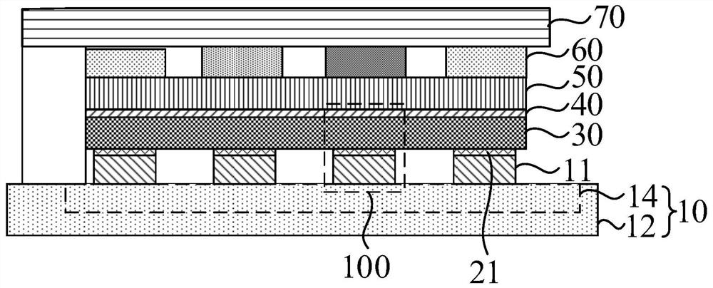
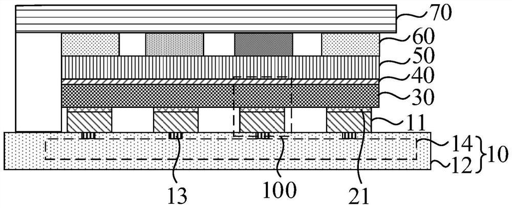
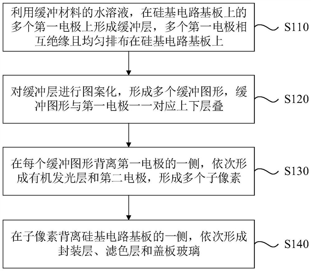
[0052] The present invention will be further described in detail below in conjunction with the accompanying drawings and embodiments. It should be understood that the specific embodiments described here are only used to explain the present invention, but not to limit the present invention. In addition, it should be noted that, for the convenience of description, only some structures related to the present invention are shown in the drawings but not all structures.

[0053] figure 1 It is a structural schematic diagram of a silicon-based organic electroluminescence microdisplay provided by an embodiment of the present invention, refer to figure 1, the silicon-based organic electroluminescent microdisplay includes a silicon-based circuit substrate 10, the silicon-based circuit substrate 10 includes a silicon-based substrate 12 and a driver circuit 14 located on the silicon-based substrate 12; a plurality of sub-pixels 100, and the sub-pixels 100 are arranged On the silicon-bas...


PUM


Abstract

The embodiment of the invention discloses a silicon-based organic electroluminescent micro-display and a preparation method thereof. The silicon-based organic light-emitting micro display comprises asilicon-based circuit substrate, and a plurality of sub-pixels, wherein the silicon-based circuit substrate comprises a silicon-based substrate and a driving circuit positioned on the silicon-based substrate; the sub-pixels are arranged on the silicon-based circuit substrate, each sub-pixel comprises a first electrode, a buffer pattern, an organic light-emitting layer and a second electrode whichare sequentially arranged in a stacked mode, and the first electrodes are electrically connected with the driving circuit; and the buffer pattern is formed by patterning a buffer layer, and the bufferlayer is prepared from an aqueous solution of a buffer material. According to the embodiment of the invention, the problem that transverse electric leakage easily occurs between sub-pixels in an existing silicon-based organic electroluminescent micro-display is solved, color crossing between the sub-pixels can be avoided, and meanwhile, the hole injection capability of the sub-pixels can be improved, the recombination efficiency of carriers is improved, and the luminous efficiency of the sub-pixels is improved.

Description

technical field [0001] The embodiments of the present invention relate to the field of display technology, in particular to a silicon-based organic electroluminescence microdisplay and a preparation method thereof. Background technique [0002] A silicon-based organic electroluminescent device is an optoelectronic device in which an organic electroluminescent material is further fabricated on a single crystal silicon substrate prepared with a semiconductor CMOS circuit. After packaging, a silicon-based organic light-emitting microdisplay can be formed. Silicon-based organic electroluminescent display has the characteristics of brightness, rich colors, low driving voltage, fast response speed and low power consumption, and can provide higher definition resolution in a display area of ​​less than 1 inch. Therefore, it is developing very rapidly. It can be used in military, medical, industrial, aerospace, entertainment and consumer electronics fields, especially novel applicati...

Claims


Application Information

Patent Timeline
Patent Type & Authority Applications(China)
IPC IPC(8): H01L27/32H01L51/56H01L51/00
CPCH10K71/10H10K71/20H10K59/12H10K71/00
Inventor 刘玉龙沈伟星季渊潘仲光
Owner 南京昀光科技有限公司
Why Eureka
Try Eureka