Biometric feature recognition image processing device and processing method

A biometric feature recognition and image processing device technology, applied in the electronic field, can solve problems such as unsatisfactory processing methods, long processing waiting time, and long waiting time, so as to improve processing efficiency and circuit performance, and reduce complexity and confusion degree, the effect of reducing waiting time

Pending Publication Date: 2021-03-19
SHANGHAI FINGER TECH CO LTD
View PDF0 Cites 0 Cited by
  • Summary
  • Abstract
  • Description
  • Claims
  • Application Information

AI Technical Summary

Problems solved by technology

In this image processing flow, there are two most time-consuming parts. One is that most electronic devices transmit images through serial buses such as I2C, so a lot of time will be consumed in the process of image data entering; the other is The part is that image algorithm processing also takes a lot of time, especially the process of multi-algorithm processing, such as figure 1 The first algorithm processor will read data processing from SRAM, and the second algorithm processing can continue to read useful data processing from SRAM, and so on, so that processing wi

Method used


Image

  • Biometric feature recognition image processing device and processing method
  • Biometric feature recognition image processing device and processing method
  • Biometric feature recognition image processing device and processing method

Examples


Embodiment Construction

[0041] In order to make the purposes, technical solutions and advantages of the embodiments of the present application clearer, the technical solutions in the embodiments of the present application will be clearly and completely described below in conjunction with the drawings in the embodiments of the present application. Obviously, the described embodiments It is a part of the embodiments of this application, not all of them. Based on the embodiments in this application, all other embodiments obtained by persons of ordinary skill in the art without creative efforts fall within the protection scope of this application.

[0042] The technical solution of the present invention will be described in detail below with specific embodiments. The following specific embodiments may be combined with each other, and the same or similar concepts or processes may not be repeated in some embodiments.

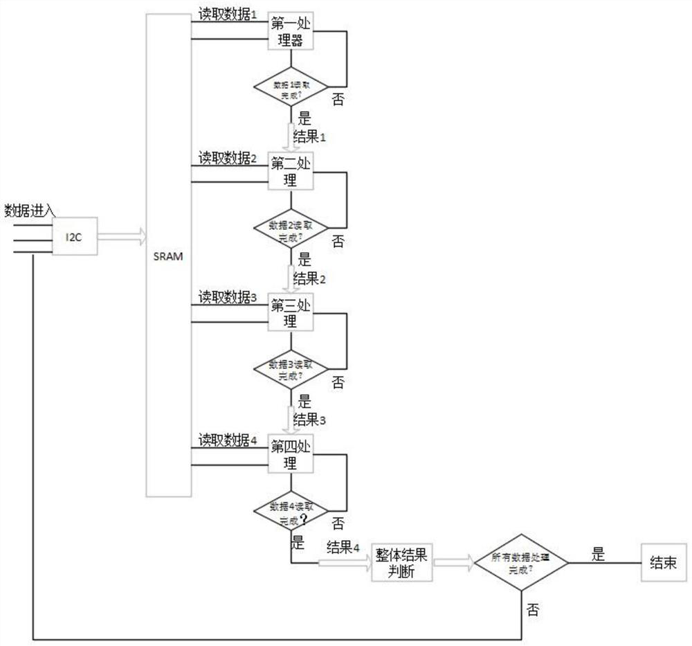
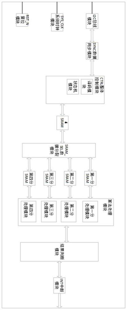
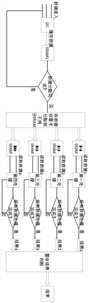
[0043] Please refer to figure 2 , figure 2 It is a schematic diagram of the circuit...


PUM


Abstract

The invention discloses a biometric feature recognition image processing device and processing method, and the device comprises: an I2C bus module which is used for configuring an instruction and receiving and transmitting external image data; a total SRAM module; a sub-SRAM module group, wherein the sub-SRAM module group comprises a first sub-SRAM module, a second sub-SRAM module, a third sub-SRAM module, a fourth sub-SRAM module... and an mth sub-SRAM module; an algorithm processing module, wherein the algorithm processing module comprises a first sub-processing module, a second sub-processing module, a third sub-processing module, a fourth sub-processing module... an mth sub-processing module; a result judgment module; and an interrupt module. The invention reduces the time of digital circuit image data processing.

Description

technical field [0001] The invention relates to the electronic field, and specifically relates to a biometric feature recognition image processing device, a biometric feature recognition image processing device, a biometric feature recognition module, and electronic equipment. Background technique [0002] In consumer electronic products such as mobile phones and computers, the use of image sensors is already essential, such as cameras, fingerprint sensors, etc. When using face recognition or fingerprint recognition for image unlocking, the unlocking time is extremely important for consumers' experience. For a large amount of image data, the commonly used processing method is that the image data enters, and then is cached by SRAM1 (static random access memory), and then the image data is analyzed and the image data is processed by an algorithm. After the processing is completed, continue to input image, the detailed steps are as figure 1 shown. In this image processing fl...

Claims


Application Information

Patent Timeline
IPC IPC(8): G06K9/00
CPCG06V40/13G06V10/955
Inventor 陈荑徐启波黄昊
Owner SHANGHAI FINGER TECH CO LTD
Why Eureka
Try Eureka