An intelligent wiring method and system for chip design

A technology of intelligent wiring and chip design, applied in computer-aided design, computing, special data processing applications, etc., can solve problems such as low efficiency and complicated methods, and achieve the effect of improving efficiency

Active Publication Date: 2022-04-19
合肥名龙电子科技有限公司
View PDF0 Cites 0 Cited by
  • Summary
  • Abstract
  • Description
  • Claims
  • Application Information

AI Technical Summary

Problems solved by technology

[0003] The purpose of the present invention is to provide an intelligent wiring method and system for chip design, which is used to solve the problems of complex methods and low efficiency in chip design

Method used


Image

  • An intelligent wiring method and system for chip design
  • An intelligent wiring method and system for chip design
  • An intelligent wiring method and system for chip design

Examples


Embodiment Construction

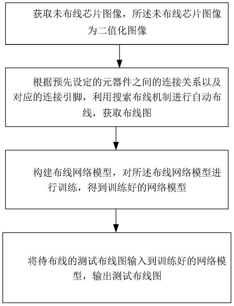
[0037] In order to make the purpose, technical solutions and advantages of the embodiments of the present invention clearer, the technical solutions in the embodiments of the present invention will be introduced below in conjunction with the drawings in the embodiments of the present invention. In order to make the object, technical solution and advantages of the present invention clearer, the present invention will be further described in detail below in conjunction with the accompanying drawings and embodiments. It should be understood that the specific embodiments described here are only used to explain the present invention, not to limit the present invention.

[0038] It should be noted that the specific scenario targeted by the present invention is the wiring scenario of chip design, that is, the wiring simulation performed during signal integrity simulation, and its object is an ideal simulation image with pre-arranged components, that is, no components If the layout is...


PUM


Abstract

The present invention relates to an intelligent wiring method and system for chip design, which is mainly through wiring the pre-arranged components, that is, first obtaining the binarized image of the unwired chip, and according to the pre-set components The connection relationship between them and the corresponding connection pins, use the search wiring mechanism to perform automatic wiring, obtain the wiring diagram, and then use the constructed neural network model to train the wiring chips, and realize the wiring of the chips to be wired; that is, in the present invention The connection between the two components can be better determined through the set search and wiring mechanism, and automatic wiring is realized. Combined with the neural network model, the wiring of a large number of chips can be realized.

Description

technical field [0001] The invention relates to an intelligent wiring method and system for chip design, belonging to the field of integrated circuit automatic wiring. Background technique [0002] With the rapid development of integrated circuit technology, integrated circuits have entered the era of ultra-deep submicron, which makes the feature size of electronic devices smaller and smaller, the scale of chips is larger and larger, and more and more components can be integrated in a single On the chip, the complexity has risen sharply, and for the wiring method in the layout, the manual design wiring method has long been unable to meet the needs of integrated circuit design, and computer automatic wiring has occupied an increasing proportion of layout design and wiring. The wiring algorithm has an extremely important impact on the speed and efficiency of wiring. How to design an algorithm that requires less time and space, lower complexity, and higher efficiency has become...

Claims


Application Information

Patent Timeline
Patent Type & Authority Patents(China)
IPC IPC(8): G06F30/3947
CPCG06F30/3947
Inventor 王丹阳卢亚鹏贺伟侯宁王新刚张伟龙丁文波刘军凯
Owner 合肥名龙电子科技有限公司
Why Eureka
Try Eureka