Automatic generation method of chip monitoring signal

A monitoring signal, automatic generation technology, applied in hardware monitoring, instrumentation, error detection/correction, etc., can solve problems such as unguaranteed efficiency and quality, time-consuming and labor-intensive, etc., to facilitate debugging and query, avoid human error, develop Efficiency improvement effect

Active Publication Date: 2021-12-24
无锡众星微系统技术有限公司
View PDF0 Cites 0 Cited by
  • Summary
  • Abstract
  • Description
  • Claims
  • Application Information

AI Technical Summary

Problems solved by technology

Because the overall structure of the chip is very complex, there are many signals and modules to be monitored, and most of the work is almost done manually, which is time-consuming and labor-intensive, and it is impossible to avoid errors in artificial design and arrangement of monitoring signals, and the efficiency and quality cannot be guaranteed.

Method used


Image

  • Automatic generation method of chip monitoring signal
  • Automatic generation method of chip monitoring signal
  • Automatic generation method of chip monitoring signal

Examples


Embodiment Construction

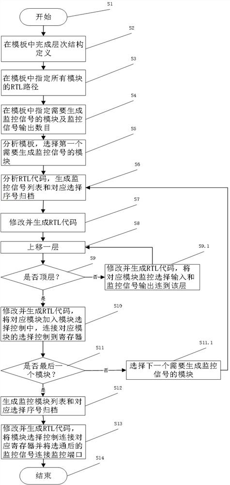
[0034] In order to make the purpose, technical solutions and advantages of the embodiments of the present invention more clear, the technical solutions in the embodiments of the present invention will be clearly and completely described below in conjunction with the accompanying drawings in the embodiments of the present invention. Obviously, the described embodiments It is a part of embodiments of the present invention, but not all embodiments. Based on the embodiments of the present invention, all other embodiments obtained by persons of ordinary skill in the art without making creative efforts belong to the protection scope of the present invention.

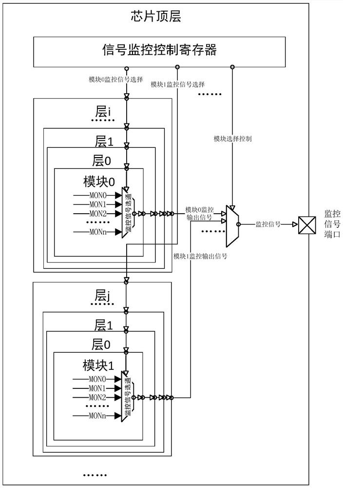
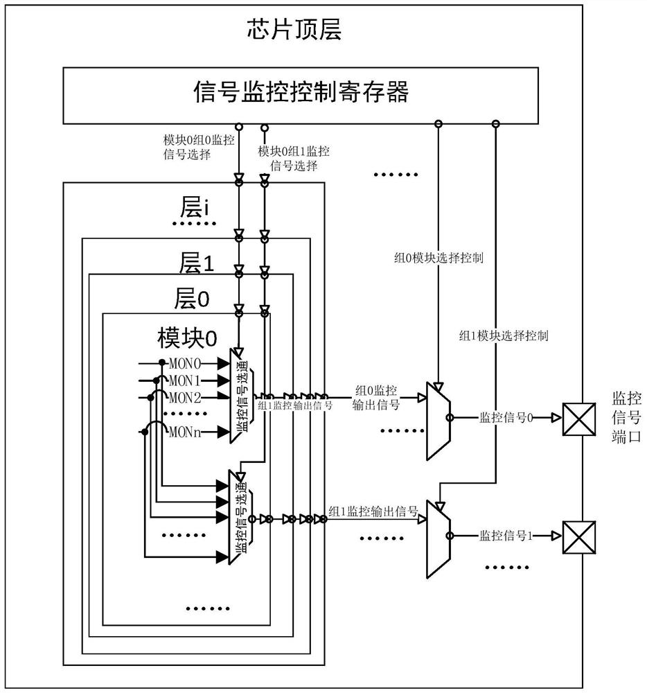
[0035] The invention provides an automatic generation method and design flow of a chip monitoring signal. After the basic information that is simple and easy to maintain is given, the basic information is extracted by using a script, and the RTL code of the specified module is analyzed. Automatically generate monitoring signal...


PUM


Abstract

The invention provides a method for automatically generating chip monitoring signals, which analyzes the hierarchical structure of the chip, extracts internal monitoring signals, and generates a list of monitoring signals; organizes and archives the monitoring signals; modifies the RTL code of the corresponding module, A port associated with the monitoring signal is generated. The invention automatically generates a chip monitoring signal by analyzing the chip module, avoids human errors in the process of generating RTL design codes, and improves chip development efficiency.

Description

technical field [0001] The invention belongs to the field of chip design, in particular to an automatic generation method of a chip monitoring signal. Background technique [0002] Monitoring signals has become an essential element in chip design and development. The monitoring signal can be introduced to observe the specified signal inside the chip. Through the monitoring signal, the internal problems and defects of the chip can be quickly and effectively analyzed and located during tape-out, which is very important for understanding the internal operation of the chip, helping the chip to improve quality, and improving yield. However, the traditional design and development methods are all aimed at the needs of the design itself. The designer of the corresponding module manually organizes and archives the monitoring signals, and modifies the corresponding RTL design. The top-level summary control is then output by the chip monitor port. Because the overall structure of th...

Claims


Application Information

Patent Timeline
Patent Type & Authority Patents(China)
IPC IPC(8): G06F11/30
CPCG06F11/3013
Inventor 张辅云刁永翔
Owner 无锡众星微系统技术有限公司
Why Eureka
Try Eureka