
Eureka
For R&D, Eureka makes reading and utilizing patents & technical documents easy.
Eureka AIR
Designed for self-driven R&D workflows. Generate viable solutions, solve complex R&D challenges, empower your innovation with AI.

Eureka Materials
Designed for material experts only. Revolutionize your material R&D, from search, analyze, to developing new materials.

TechResearch
Generate reliable direction feasibility study reports for your R&D in just a few steps.

TechSeek
Discover and master advanced knowledge NOW. Basics, ideas, possibilities, all at once.

TechMind
As an expert in R&D Theories, TechMind can generates customized viable solutions instantly.

TechRisk
Analyze your overall solution with one click, know your potential R&D risks in advance.

TechMonitor
Get weekly tech updates, stay abreast of the latest tech innovations and key insights.
Optical imaging lens and imaging equipment
A technology of optical imaging lens and imaging surface, which is applied in the field of imaging lens, can solve the problems of many aspherical lenses and high production cost, and achieve the effects of good imaging quality, convenient assembly, and large aperture assembly
- Summary
- Abstract
- Description
- Claims
- Application Information
AI Technical Summary
Problems solved by technology
Method used
Image

Examples
no. 1 example
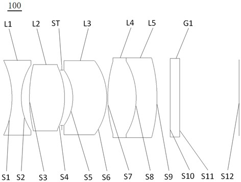
[0064] see figure 1 , which is a schematic structural view of the optical imaging lens 100 provided in the first embodiment of the present invention, the optical imaging lens 100 includes in sequence from the object side to the imaging surface along the optical axis: a first lens L1, a second lens L2, and a diaphragm ST, the third lens L3, the fourth lens L4, the fifth lens L5, and the filter G1;
[0065] The first lens L1 has negative refractive power, and the object side S1 of the first lens and the image side S2 of the first lens are both concave surfaces;
[0066] The second lens L2 has positive refractive power, and the object side S3 of the second lens and the image side S4 of the second lens are both convex surfaces;
[0067] The third lens L3 has positive refractive power, the object side S5 of the third lens is concave, and the image side S6 of the third lens is convex;
[0068] The fourth lens L4 has a positive refractive power, and the object side S7 of the fourth...
no. 2 example
[0079] The structure of the optical imaging lens provided by the second embodiment of the present invention is substantially the same as that of the optical imaging lens 100 provided by the first embodiment, except that the parameters such as radius of curvature, thickness, and material selection of each lens are different.
[0080] Please refer to Table 2, which shows the relevant parameters of each lens in the optical imaging lens provided by the second embodiment of the present invention.
[0081] Table 2
[0082]
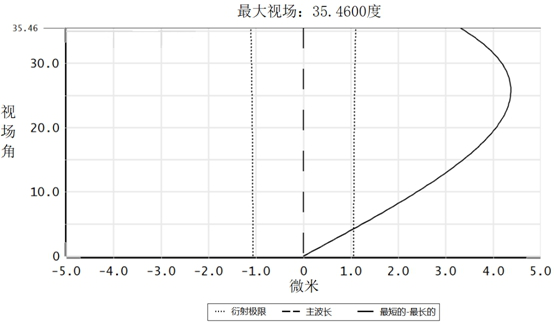
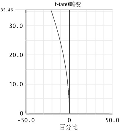
[0083] Please refer to Figure 5 , Image 6 with Figure 7 , respectively show the vertical axis chromatic aberration diagram, distortion curve diagram and relative illuminance diagram of the optical imaging lens in this embodiment. from Figure 5 It can be seen from the figure that the difference between short-wave chromatic aberration and long-wave chromatic aberration is controlled within 3.5 microns, indicating that the vertical axis chromatic aberrat...
no. 3 example
[0088] see Figure 8 , shows the imaging device 300 provided by the third embodiment of the present invention, and the imaging device 300 may include an imaging element 310 and the optical imaging lens (such as the optical imaging lens 100 ) in any of the above embodiments. The imaging element 310 may be a CMOS (Complementary Metal Oxide Semiconductor, Complementary Metal Oxide Semiconductor) image sensor, and may also be a CCD (Charge Coupled Device, Charge Coupled Device) image sensor.
[0089] The imaging device 300 may be a vehicle-mounted camera, a surveillance camera, or any other form of electronic device loaded with the aforementioned optical imaging lens.
[0090] The imaging device 300 provided in the embodiment of the present application includes an optical imaging lens 100. Since the optical imaging lens 100 has the advantages of large image area, large aperture and high illuminance, the imaging device 300 with the optical imaging lens 100 also has a large image ar...
PUM
 Abstract
Description
Claims
Application Information
 - R&D Engineer
- R&D Manager
- IP Professional
- Industry Leading Data Capabilities
- Powerful AI technology
- Patent DNA Extraction
Browse by: Latest US Patents, China's latest patents, Technical Efficacy Thesaurus, Application Domain, Technology Topic, Popular Technical Reports.
© 2024 PatSnap. All rights reserved.Legal|Privacy policy|Modern Slavery Act Transparency Statement|Sitemap|About US| Contact US: help@patsnap.com