Manufacturing method of memory address line

A technology of memory address and manufacturing method, which is applied in the semiconductor field

Pending Publication Date: 2021-08-24
YANGTZE ADVANCED MEMORY INDUSTRIAL INNOVATION CENTER CO LTD
View PDF5 Cites 0 Cited by
  • Summary
  • Abstract
  • Description
  • Claims
  • Application Information

AI Technical Summary

Problems solved by technology

[0003] In the related art, there are many problems when forming the address lines in the memory with high distribution density

Method used


Image

  • Manufacturing method of memory address line
  • Manufacturing method of memory address line
  • Manufacturing method of memory address line

Examples


Embodiment Construction

[0060] In order to make the technical solutions and advantages of the embodiments of the present invention more clear, the specific technical solutions of the invention will be further described in detail below in conjunction with the drawings in the embodiments of the present invention. The following examples are used to illustrate the present invention, but are not intended to limit the scope of the present invention.

[0061] In the following paragraphs the invention is described more specifically by way of example with reference to the accompanying drawings. Advantages and features of the present invention will be apparent from the following description and claims. It should be noted that all the drawings are in a very simplified form and use imprecise scales, and are only used to facilitate and clearly assist the purpose of illustrating the embodiments of the present invention.

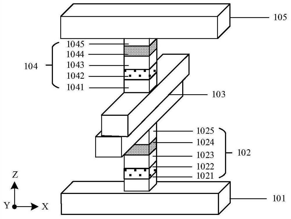
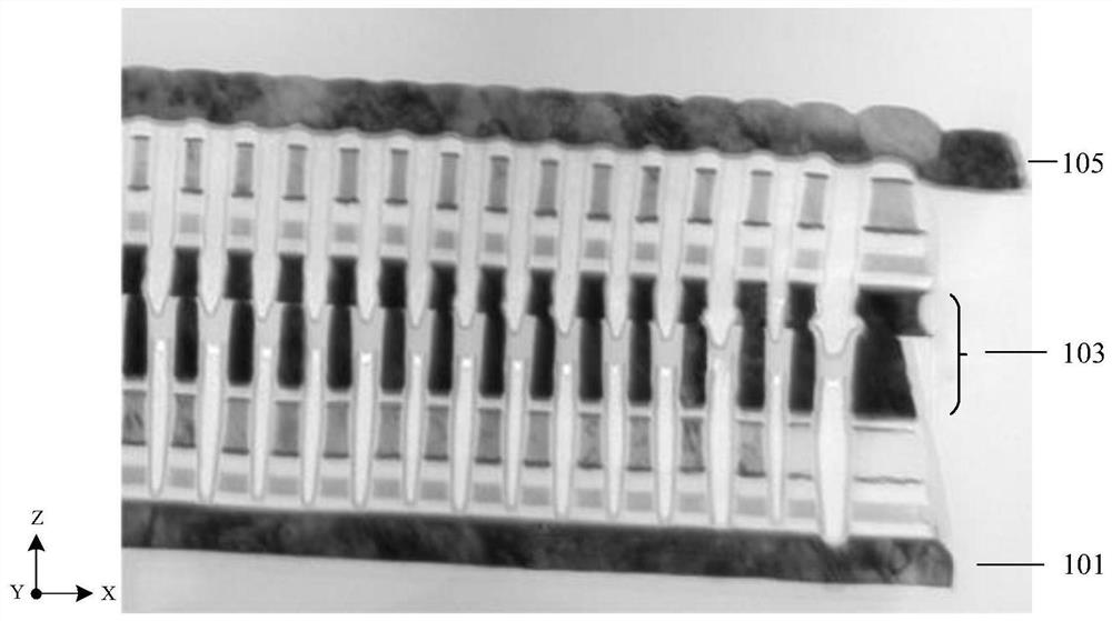
[0062]The memory involved in the embodiment of the present invention may include a memory co...


PUM


Abstract

The embodiment of the invention provides a manufacturing method of a memory address line. The manufacturing method comprises the following steps of providing a semiconductor structure, wherein the semiconductor structure at least comprises a first address line layer; forming a first sacrificial layer on the first address line layer; performing first etching on the first sacrificial layer to form a plurality of first sacrificial strips which extend along a first direction and are spaced by a first distance; forming a first directional assembly layer, wherein the first directional assembly layer comprises a plurality of second sacrificial strips and first medium strips which are arranged at intervals; the plurality of second sacrifice strips extend along the first direction and are spaced by a second distance; the second distance is smaller than the first distance; and partial second sacrificial strips in the plurality of second sacrificial strips are overlapped with the projections of the plurality of first sacrificial strips on a first plane perpendicular to the first direction; removing the first dielectric strips; and performing second etching on the first address line layer by using the second sacrificial strip as a first mask layer to obtain a first address line.

Description

technical field [0001] Embodiments of the present invention relate to the technical field of semiconductors, and in particular to a method for manufacturing memory address lines. Background technique [0002] With the continuous development of the information society, the demand for high-density memory in various industries is increasing. Therefore, in order to increase the storage density of the memory, the distribution density of the address lines (word lines and bit lines) in the memory is generally designed to be relatively high, that is, The gap between word lines or bit lines is very small. [0003] In the related art, there are many problems when forming address lines in a memory with a relatively high distribution density. Contents of the invention [0004] In order to solve related technical problems, an embodiment of the present invention proposes a method for manufacturing memory address lines. [0005] An embodiment of the present invention provides a method ...

Claims


Application Information

Patent Timeline
Patent Type & Authority Applications(China)
IPC IPC(8): H01L27/24
CPCH10B63/84H10B63/80
Inventor 刘峻杨红心
Owner YANGTZE ADVANCED MEMORY INDUSTRIAL INNOVATION CENTER CO LTD
Why Eureka
Try Eureka