Semiconductor packaging device and manufacturing method thereof

A packaging device, semiconductor technology, applied in the direction of semiconductor/solid-state device manufacturing, semiconductor devices, semiconductor/solid-state device components, etc., can solve the problems of occupying a certain space, occupying a large space, and a large area.

Pending Publication Date: 2021-09-10
ADVANCED SEMICON ENG INC
View PDF0 Cites 0 Cited by
  • Summary
  • Abstract
  • Description
  • Claims
  • Application Information

AI Technical Summary

Problems solved by technology

However, the iron cover itself needs to occupy a certain space in the thickness of the product (also called the height, or the Z direction), and due to the influence of the process technology of placing the iron cover in the product, it is necessary to reserve a certain space around the iron cover , which ultimately leads to the iron cover occupying a large area in the plane direction (also called the

Method used


Image

  • Semiconductor packaging device and manufacturing method thereof
  • Semiconductor packaging device and manufacturing method thereof
  • Semiconductor packaging device and manufacturing method thereof

Examples


Embodiment Construction

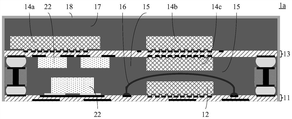
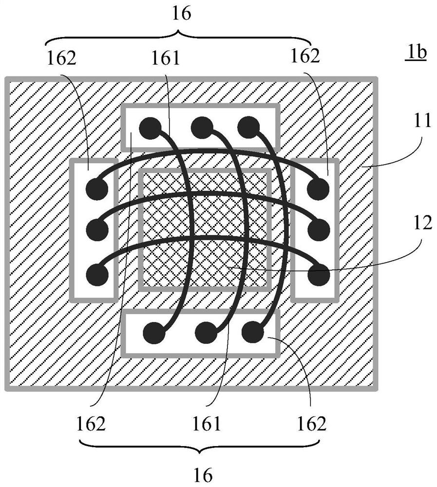
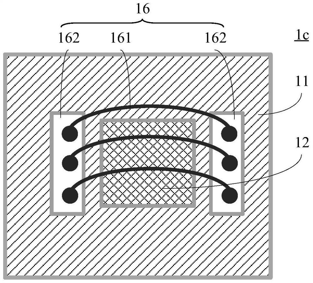
[0045] The specific implementation of the present invention will be described below in conjunction with the accompanying drawings and examples. Those skilled in the art can easily understand the technical problems solved by the present invention and the technical effects produced by the content recorded in this specification. It should be understood that the specific embodiments described here are only used to explain related inventions, rather than to limit the invention. In addition, for the convenience of description, only the parts related to the related invention are shown in the drawings.

[0046] It should be noted that the structures, proportions, sizes, etc. shown in the accompanying drawings of the specification are only used to match the content recorded in the specification for the understanding and reading of those skilled in the art, and are not intended to limit the implementable aspects of the present invention. Limiting conditions, so there is no technical sub...


PUM


Abstract

The invention provides a semiconductor packaging device and a manufacturing method thereof. According to the invention, a routing shielding structure is adopted to replace a traditional iron cover for signal shielding, so that the plane area occupation of a semiconductor packaging device can be reduced, and the overall height can be reduced; and high temperature is not needed in the routing process, so that the semiconductor packaging device and the manufacturing method thereof can be more suitable for products sensitive to temperature.

Description

technical field [0001] The present disclosure relates to the technical field of semiconductor packaging, in particular to a semiconductor packaging device and a manufacturing method thereof. Background technique [0002] In order to meet the requirement of internal electromagnetic signal shielding in a 3D (3 dimension, three-dimensional) structure with upper and lower substrates, most iron covers are currently used to implement signal shielding. However, the iron cover itself needs to occupy a certain space in the thickness of the product (also called the height, or the Z direction), and due to the influence of the process technology of placing the iron cover in the product, it is necessary to reserve a certain space around the iron cover , which eventually leads to the iron cover occupying a large area in the plane direction (also called the X / Y direction), which in turn leads to a large space occupied by the iron cover used as a signal shield in the overall product, that i...

Claims


Application Information

Patent Timeline
IPC IPC(8): H01L23/31H01L23/552H01L25/16H01L21/50H01L21/56
CPCH01L23/552H01L23/3121H01L25/162H01L21/50H01L21/56
Inventor 陈昱敞张维栋
Owner ADVANCED SEMICON ENG INC
Why Eureka
Try Eureka