
Display device and electronic equipment

A display device and display area technology, which is applied in the direction of circuits, electrical components, and electric solid devices, can solve problems affecting image display quality, etc., and achieve the effects of improving image display quality, solving leakage current, and solving abnormal display

Pending Publication Date: 2022-01-07
WUHAN TIANMA MICRO ELECTRONICS CO LTD
View PDF0 Cites 0 Cited by
  • Summary
  • Abstract
  • Description
  • Claims
  • Application Information

AI Technical Summary

Problems solved by technology

However, the conventional under-screen design structure of the optical fingerprint recognition chip will affect the image display quality

Method used


Image

  • Display device and electronic equipment
  • Display device and electronic equipment
  • Display device and electronic equipment

Examples


Embodiment Construction

[0027] The following will clearly and completely describe the embodiments of the present application with reference to the drawings in the embodiments of the present application. Obviously, the described embodiments are only some of the embodiments of the present application, not all of them. Based on the embodiments in this application, all other embodiments obtained by persons of ordinary skill in the art without making creative efforts belong to the scope of protection of this application.

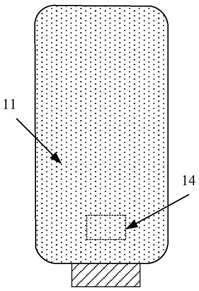
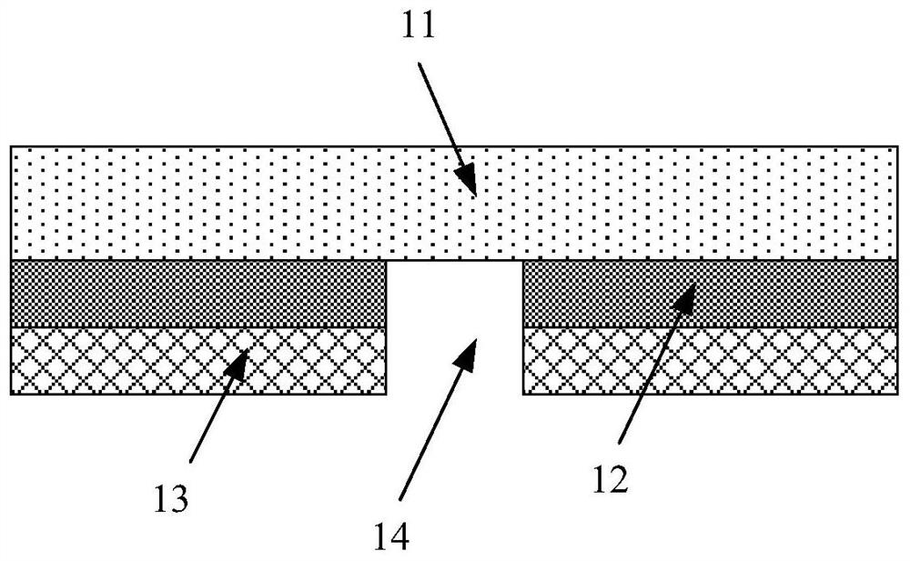
[0028] Such as figure 1 and figure 2 as shown, figure 1 It is a top view of a display device that can be adapted to the design of an optical fingerprint recognition chip under the screen, figure 2 for figure 1 The cutaway view of the display device shown includes: a display panel 11 with a supporting layer 12 and a protective layer 13 . The supporting layer 12 is located on a side away from the display surface of the display panel 11 , and is located between the display panel 11 a...


PUM

PropertyMeasurementUnit
Thickness rangeaaaaaaaaaa

Abstract

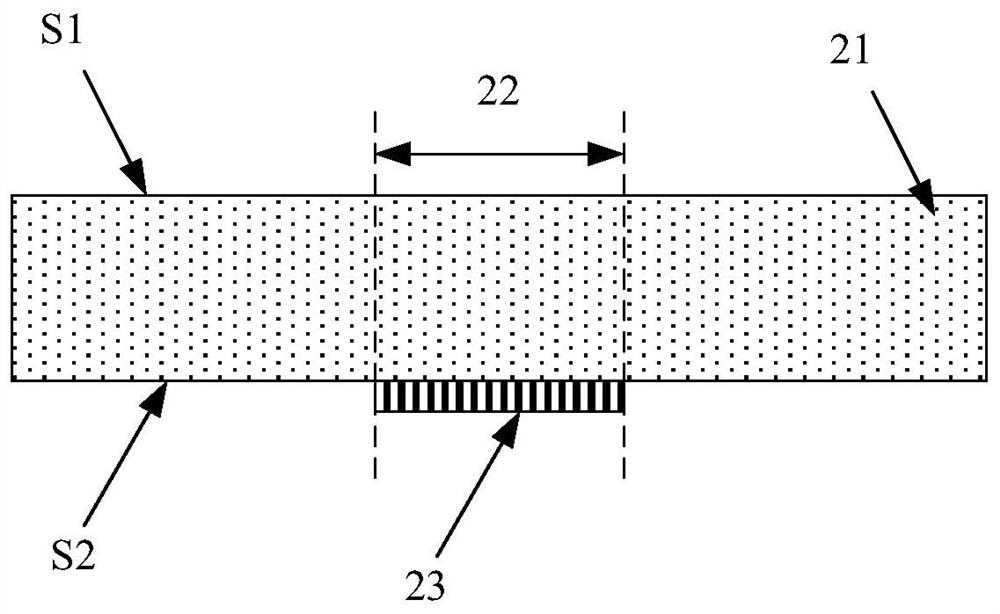
The invention discloses a display device and electronic equipment. The display device comprises a display panel, and a function layer; the display panel is provided with a first surface and a second surface which are oppositely arranged, the first surface is a display surface, and at least part of the display surface is a fingerprint acquisition area; the function layer is arranged on the second surface, and the vertical projection of the function layer on the first surface is at least partially overlapped with the fingerprint acquisition area; and the functional layer is used for reducing total reflection of light on the second surface towards the interior of the display panel. According to the display device of the technical schemes, the functional layer is arranged on the second surface of the display panel, the vertical projection of the functional layer on the first surface is at least partially overlapped with the fingerprint collection area, and the functional layer can reduce total reflection of the light rays towards the interior of the display panel on the second surface, so that the problem that a channel layer in a TFT (Thin Film Transistor) in the display panel senses the light rays to cause leakage current after the light rays enters the display panel is solved, the display abnormity caused by the leakage current is solved, and the image display quality is improved.

Description

technical field [0001] The present application relates to the technical field of electronic equipment, and more specifically, to a display device and electronic equipment. Background technique [0002] With the continuous advancement of science and technology, more and more electronic devices are widely used in people's daily life and work, bringing great convenience to people's daily life and work, and becoming an indispensable and important tool for people today. tool. [0003] The main component of electronic equipment to realize the display function is the display panel. In order to realize the safe and convenient identification function, a fingerprint identification chip can be integrated in the electronic equipment. Among them, the optical fingerprint identification chip is one of the mainstream fingerprint identification chips at that time. [0004] When an optical fingerprint recognition chip is integrated in an electronic device, in order to realize a full screen, ...

Claims


Application Information

Patent Timeline
IPC IPC(8): H01L27/32G06K9/00
CPCH10K59/12
Inventor 熊鑫王永志彭涛
Owner WUHAN TIANMA MICRO ELECTRONICS CO LTD
Learn More