Array substrate, manufacturing method thereof and display panel

A technology of array substrates and substrate substrates, which is applied in semiconductor/solid-state device manufacturing, instruments, semiconductor devices, etc., can solve problems such as signal attenuation of metal signal lines, abnormal screen display, etc., and achieve the effect of solving display abnormalities and improving display quality

Pending Publication Date: 2022-08-05
CHONGQING HKC OPTOELECTRONICS TECH CO LTD +1
View PDF0 Cites 0 Cited by
  • Summary
  • Abstract
  • Description
  • Claims
  • Application Information

AI Technical Summary

Problems solved by technology

[0004] The present application provides an array substrate, its manufacturing method, and a display panel, at least solving the problem of abnormal picture display caused by signal attenuation of metal signal lines

Method used


Image

  • Array substrate, manufacturing method thereof and display panel
  • Array substrate, manufacturing method thereof and display panel
  • Array substrate, manufacturing method thereof and display panel

Examples


no. 1 example

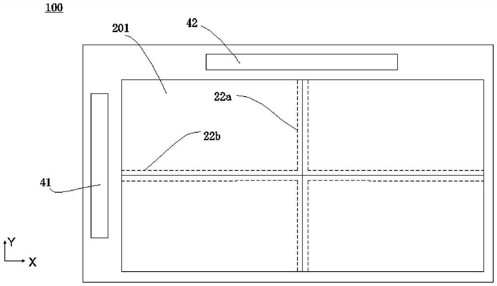
[0054] A first embodiment of the first aspect of the present application provides an array substrate. Please refer to Figure 1 to Figure 5 , the array substrate 100 includes a base substrate 10 , a display circuit 20 and an auxiliary circuit 30 disposed on the base substrate 10 .

[0055] The base substrate 10 includes a first surface 11 and a second surface 12 disposed opposite to each other, and a plurality of through holes 13 penetrating the first surface 11 and the second surface 12 are provided on the base substrate 10 .

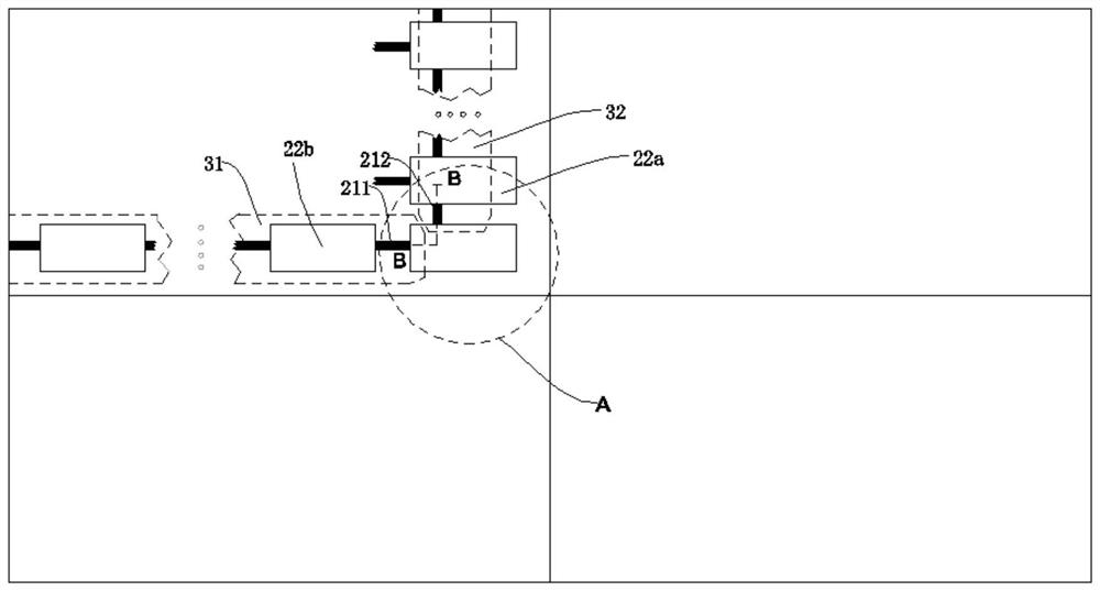
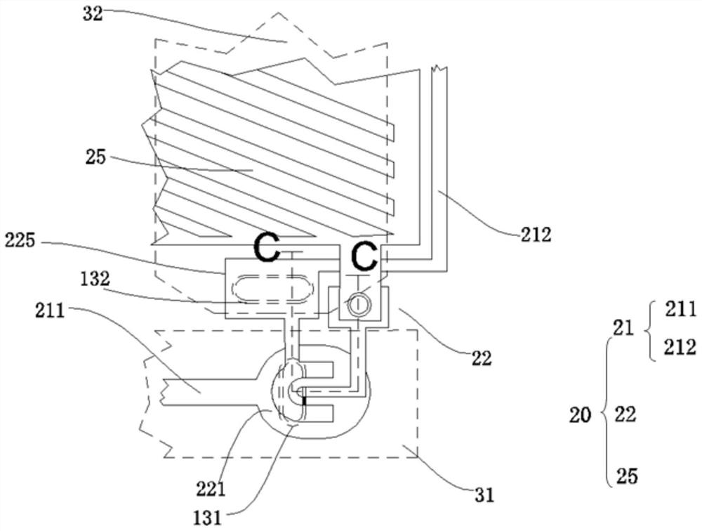
[0056] The display line 20 is disposed on the first surface 11 , and the display line 20 includes a signal line 21 connected with the driving circuit and a thin film transistor (TFT) 22 connected with the signal line 21 . The display circuit 20 is used for transmitting the driving signal provided by the driving circuit to the thin film transistor 22 , so as to control the on-off of the thin film transistor 22 and provide a preset voltage to the thin f...

no. 2 example

[0085] A second embodiment of the second aspect of the present application provides a method for manufacturing an array substrate. Please refer to Figure 1 to Figure 6 , the manufacturing method of the array substrate includes the following steps.

[0086] Step S110 : providing a base substrate 10 , the base substrate 10 includes a first surface 11 and a second surface 12 disposed opposite to each other.

[0087] The base substrate 10 may be a transparent glass substrate, but is not limited thereto.

[0088] Step S120 : forming the display circuit 20 on the first surface 11 .

[0089] The display line 20 includes a signal line 21 and a thin film transistor 22 connected to the signal line 21; the signal line 21 has a proximal end close to the driving circuit and a distal end far away from the driving circuit.

[0090] Specifically, the signal line 21 includes a scan line 211 for connecting the gate driving unit 41 and a data line 212 for connecting the data driving unit 42;...

no. 3 example

[0121] A third embodiment of the third aspect of the present application provides a display panel. Please refer to Figure 12 The display panel 1 includes the array substrate 100 according to the first aspect, the opposite substrate 200 disposed opposite to the array substrate 100, and the liquid crystal layer 300 disposed between the array substrate 100 and the opposite substrate 200, wherein the opposite substrate 200 can be It is a color filter substrate provided with a color filter film, but is not limited thereto. For example, a color filter film can also be provided on the array substrate 100 .

[0122] The above-mentioned display panel 1 solves the problems of abnormal picture display and splicing slits caused by signal attenuation of metal signal lines.


PUM

PropertyMeasurementUnit
widthaaaaaaaaaa

Abstract

The invention is suitable for the technical field of display, and provides an array substrate which comprises a substrate, the substrate comprises a first surface and a second surface which are oppositely arranged, and a plurality of through holes penetrating through the first surface and the second surface are formed in the substrate; the array substrate further comprises a display circuit arranged on the first surface, and the display circuit comprises a signal line connected with the driving circuit and a thin film transistor connected with the signal line. The signal line is provided with a near end close to the driving circuit and a far end far away from the driving circuit; the auxiliary circuit is arranged on the second surface and connected to the driving circuit, the impedance of the back circuit is smaller than that of the signal line, and the back circuit is further connected with at least one thin film transistor arranged at the far end of the signal line through a through hole. The invention further provides a manufacturing method of the array substrate and a display panel. The problem of abnormal picture display caused by signal attenuation of the metal signal line is solved.

Description

technical field [0001] The present application belongs to the field of display technology, and in particular, relates to an array substrate, a manufacturing method thereof, and a display panel. Background technique [0002] With the development of optoelectronic display technology and semiconductor manufacturing technology, Thin Film Transistor-Liquid Crystal Display (TFT-LCD) has become the current flat-panel display by virtue of its advantages of thinness, energy saving, high display quality, and mature and stable production process. Display mainstream technology, widely used in home appliances, computers, transportation, medical and other fields. TFT-LCD mainly includes an array (Array) substrate and a color filter (Color Filter, referred to as CF) substrate, and a liquid crystal layer (Liquid Crystal Layer, referred to as LCL) disposed between the array substrate and the color filter substrate, wherein the array substrate belongs to In the core part of the display panel...

Claims


Application Information

Patent Timeline
Patent Type & Authority Applications(China)
IPC IPC(8): H01L27/12H01L21/77G02F1/1368G02F1/1362
CPCH01L27/124H01L27/1259G02F1/1362G02F1/136286G02F1/1368
Inventor 鲜济遥袁海江
Owner CHONGQING HKC OPTOELECTRONICS TECH CO LTD
Why Eureka
Try Eureka