PCB surface thin layer quality analysis method

A quality analysis, thin-layer technology, applied in the analysis of materials, material analysis using wave/particle radiation, material analysis using the measurement of secondary emissions, etc., can solve time-consuming, complicated process, contact with chemical solutions, mechanical stress and other problems. Impurity pollution and other issues

Pending Publication Date: 2022-01-14
GUANGZHOU TERMBRAY ELECTRONICS TECH CO LTD
View PDF9 Cites 2 Cited by
  • Summary
  • Abstract
  • Description
  • Claims
  • Application Information

AI Technical Summary

Problems solved by technology

[0005] The purpose of the present invention is to provide a method for analyzing the quality of a PCB surface thin layer, which is equipped with a double-beam scanning electron microscope for processing and testing the sample, which can avoid the influence of contact with chemical solutions, mechanical stress, and impurity pollution during the sample preparation process. The optimization of the test angle of the beam scanning electron microscope can achieve a nearly vertical test effect, so as to obtain accurate measurement results, so that a series of tests can be completed quickly, and the traditional analysis method is time-consuming, complicated and easily caused by test distortion. The problem

Method used


Image

  • PCB surface thin layer quality analysis method
  • PCB surface thin layer quality analysis method

Examples


Embodiment 1

[0029] A method for analyzing the quality of a PCB surface thin layer, comprising the following steps:

[0030] S1. Sample sampling: Use scissors, automatic sampler or nail scissors to take out the required measurement area from the PCB board, and use a high-pressure air gun to clean the surface. The test area needs to be as close to the edge of the sample as possible. The distance from the edge of the sample is less than 2mm;

[0031] S2. Gold spray treatment: the surface of the sample needs to be treated with conductivity, and the thickness of the gold spray is within 5 nanometers;

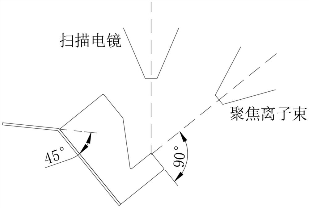
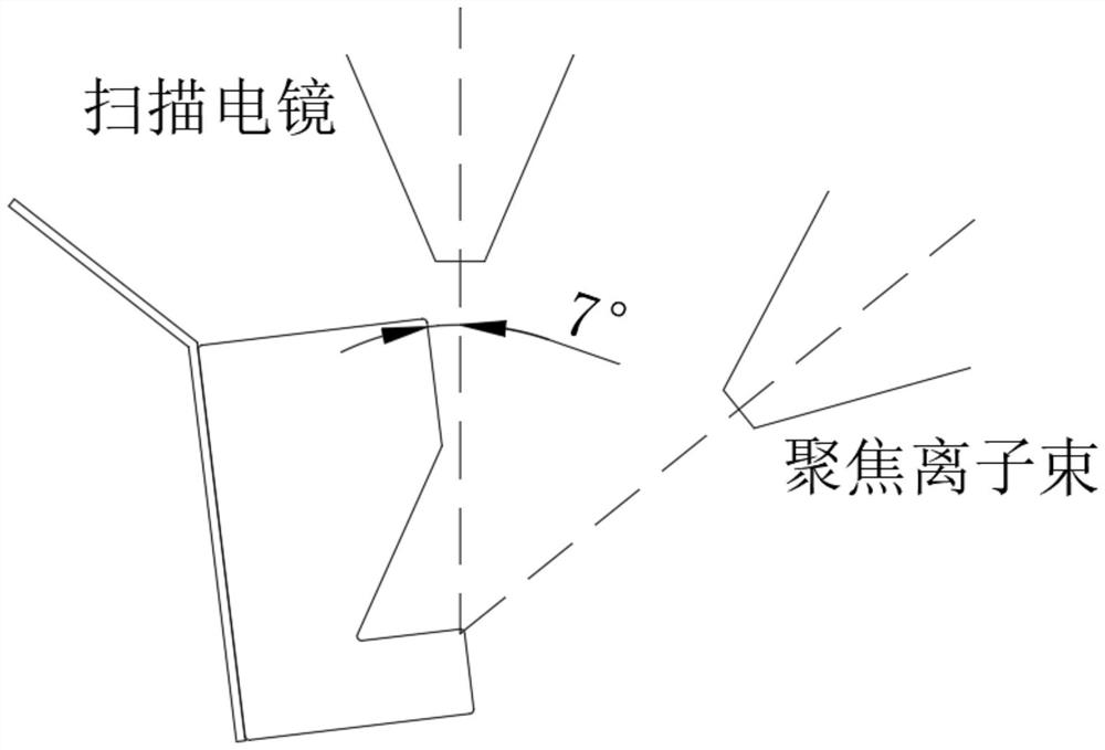
[0032] S3. Sample fixation and transfer: The sample to be tested should be firmly fixed on the metal sample stage, and ensure that the surface of the sample and the metal sample stage are well-conducted, and then install the sample stage with the sample on the inclined surface of the test platform. The area must face the highest point of the sample test platform, and the angle of the slope of t...

Embodiment 2

[0038] A method for analyzing the quality of a PCB surface thin layer, comprising the following steps:

[0039] S1. Sample sampling: Use scissors, automatic sampler or nail scissors to take out the required measurement area from the PCB board, and use a high-pressure air gun to clean the surface. The test area needs to be as close to the edge of the sample as possible. The distance from the edge of the sample is less than 2mm;

[0040] S2. Gold spray treatment: the surface of the sample needs to be treated with conductivity, and the thickness of the gold spray is within 5 nanometers;

[0041] S3. Sample fixation and transfer: The sample to be tested should be firmly fixed on the metal sample stage, and ensure that the surface of the sample and the metal sample stage are well-conducted, and then install the sample stage with the sample on the inclined surface of the test platform. The area must face the highest point of the sample test platform, and the angle of the slope of t...

Embodiment 3

[0047] A method for analyzing the quality of a PCB surface thin layer, comprising the following steps:

[0048] S1. Sample sampling: Use scissors, automatic sampler or nail scissors to take out the required measurement area from the PCB board, and use a high-pressure air gun to clean the surface. The test area needs to be as close to the edge of the sample as possible. The distance from the edge of the sample is less than 2mm;

[0049] S2. Gold spray treatment: the surface of the sample needs to be treated with conductivity, and the thickness of the gold spray is within 5 nanometers;

[0050] S3. Sample fixation and transfer: The test sample should be firmly fixed on the metal sample stage, and ensure that the surface of the sample and the metal sample stage are well-conducted, and then install the sample stage with the sample on the inclined surface of the test platform. The area must face the highest point of the sample test platform, and the angle of the slope of the measu...


PUM

PropertyMeasurementUnit
thicknessaaaaaaaaaa

Abstract

The invention discloses a PCB surface thin layer quality analysis method. The method comprises the following steps: taking out an area to be measured from the PCB by using scissors and an automatic sampler; performing metal spraying treatment; fixing a test sample on the metal sample table, and then mounting the sample table on the inclined surface of the test platform; depositing a first protective layer by using electron beams; after electron beam deposition is completed, depositing a second protective layer through a focused ion beam; adjusting the inclination angle of the measuring platform to ensure that the surface of the sample can be cut in the direction perpendicular to the focused ion beam; after cutting is completed, adjusting the inclination angle of the sample for observation. According to the invention, the sample is processed and tested by the double-beam scanning electron microscope, so that the influence of contact with a chemical solution, mechanical stress, impurity pollution and the like in the sample preparation process can be avoided, and by optimizing the test angle of the double-beam scanning electron microscope, an approximately vertical observation effect can be achieved, so that an accurate measurement result is obtained, and thus a series of tests can be completed quickly.

Description

technical field [0001] The invention relates to the technical field of PCB surface thin layer analysis, in particular to a PCB surface thin layer quality analysis method. Background technique [0002] With the continuous improvement of science and technology and the continuous upgrading of electronic products, PCB is required to develop in the direction of "high, precise and sharp". , Gold finger, OSP and other process coatings tend to become thinner and thinner, so new requirements are put forward for analyzing the quality of these thin coatings. At the same time, whether there are pollutants on the surface, and the analysis of the thickness composition after pollution are urgently needed to be resolved. [0003] Existing methods for analyzing the quality of thin surface layers: the current analysis methods are mainly through electroplating or chemical deposition of a layer of nickel (generally greater than 3 μm) or protection of the surface layer, and then making vertical...

Claims


Application Information

Patent Timeline
Patent Type & Authority Applications(China)
IPC IPC(8): G01N23/22G01N23/2202
CPCG01N23/22G01N23/2202G01N23/2251G01N2223/418G01N2223/61G01N2223/6113G01N2223/072G01N2223/081G01N23/2255G01N23/2208G01N1/28
Inventor 郑剑罗国金
Owner GUANGZHOU TERMBRAY ELECTRONICS TECH CO LTD
Why Eureka
Try Eureka