Liquid crystal display panel and 3D display device

A technology of liquid crystal display panels and display areas, applied in nonlinear optics, instruments, optics, etc., can solve the problems of liquid crystal display panels prone to moiré, and achieve the effect of eliminating moiré

Pending Publication Date: 2022-03-01
BOE TECH GRP CO LTD
View PDF0 Cites 0 Cited by
  • Summary
  • Abstract
  • Description
  • Claims
  • Application Information

AI Technical Summary

Problems solved by technology

[0005] The present invention provides a liquid crystal display panel and a 3D display device to solve the above-mentioned technical problem in the prior art that the liquid crystal display panel is prone to moiré when it is used for 3D display

Method used


Image

  • Liquid crystal display panel and 3D display device
  • Liquid crystal display panel and 3D display device
  • Liquid crystal display panel and 3D display device

Examples


Embodiment 1

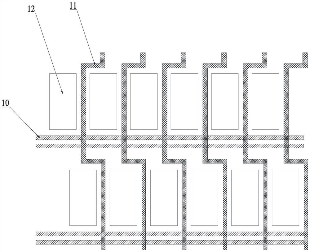
[0043] see image 3 and Figure 4 , the liquid crystal display device provided by this embodiment includes a plurality of rows of sub-pixels; in each row of sub-pixels, each sub-pixel has an effective display area, and between the effective display areas of any two adjacent sub-pixels there is a wiring area, and the wiring area is Gate lines 10 and data lines 11 are arranged, as well as other signal lines.

[0044]A liquid crystal display panel generally includes an array substrate, a color filter substrate, and a liquid crystal layer between the array substrate and the color filter substrate; on the array substrate, such as image 3 As shown, each sub-pixel area includes an open area 12 and a non-open area. The open area 12 can transmit light for display, while the non-open area is generally used for arranging gate lines 10, data lines 11 and other wirings and structures such as thin film transistors. It cannot transmit light and cannot be used for display. However, in thi...

Embodiment 2

[0057] In this embodiment, the same as the above-mentioned Embodiment 1, the liquid crystal display panel also includes multiple rows of sub-pixels, each sub-pixel has an effective display area, and has a wiring area between adjacent sub-pixels, such as Figure 10 shown. However, as far as the sub-pixels are concerned, the difference between this embodiment and the above-mentioned Embodiment 1 is that the effective display area of ​​each sub-pixel is the opening area 12 of the sub-pixel on the array substrate. That is to say, in this embodiment, the common electrode 20 is a transparent electrode; or even if the common electrode 20 is made of an opaque material, the projection of the opening 21 corresponding to each sub-pixel on the common electrode 20 on the array substrate should include The opening area 12 of the sub-pixel on the array substrate, in other words, the common electrode 20 does not play a role in shielding each sub-pixel.

[0058] see Figure 10 , in this embo...


PUM


Abstract

The invention relates to a liquid crystal display panel and a 3D display device. The liquid crystal display panel comprises a plurality of rows of sub-pixels; in each row of sub-pixels, each sub-pixel is provided with an effective display area, and a wiring area is arranged between the effective display areas of any two adjacent sub-pixels; m adjacent rows of sub-pixels are taken as a group; in any group, the area corresponding to at least one of the other (m-1) rows of sub-pixels in the group at any position of the wiring area between the effective display areas of any two adjacent sub-pixels in one row is the effective display area of the sub-pixels. The 3D display device comprises the liquid crystal display panel. According to the liquid crystal display panel, continuous display in the row direction can be achieved, and the moire phenomenon can be improved or eliminated during 3D display.

Description

technical field [0001] The present invention relates to the field of display technology, and in particular, to a liquid crystal display panel and a 3D display device. Background technique [0002] For liquid crystal display panels, such as figure 1 As shown, it includes multiple rows of gate lines (not shown in the figure) and multiple columns of data lines 2, and multiple rows of gate lines and multiple columns of data lines 2 are criss-crossed to form a grid area distributed in an array. The grid area can be used as a sub-pixel 1. In the area of ​​each sub-pixel 1, there will be traces such as gate lines and data lines, and structures such as thin film transistors (not shown in the figure) will also be formed. In the grid area, other areas except these structures can be transparent Light, that is, the open area that is actually used for display. It can be seen that, for adjacent sub-pixels, the actual display areas of the two have opaque structures, mainly gate lines, d...

Claims


Application Information

Patent Timeline
Patent Type & Authority Applications(China)
IPC IPC(8): G02F1/1343G02F1/1362
CPCG02F1/134309G02F1/134345G02F1/136286
Inventor 韩佳慧刘立伟张晨阳李付强梁蓬霞
Owner BOE TECH GRP CO LTD
Why Eureka
Try Eureka