Manufacturing method of NOR flash memory device
A flash memory device and manufacturing method technology, applied in semiconductor/solid-state device manufacturing, electric solid-state devices, semiconductor devices, etc., can solve the problem that the thickness of the side wall is not easy to control, etc.
- Summary
- Abstract
- Description
- Claims
- Application Information
AI Technical Summary
Problems solved by technology
Method used
Image

Examples
Embodiment Construction
[0030] The invention will be described below with reference to the accompanying drawings.
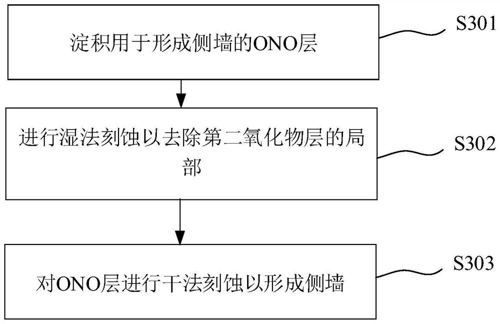
[0031] This embodiment provides a method of fabricating one or non-flash memory device. Refer figure 2 The method of making the or non-flash memory device includes the following steps:
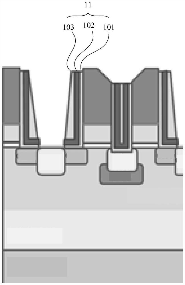
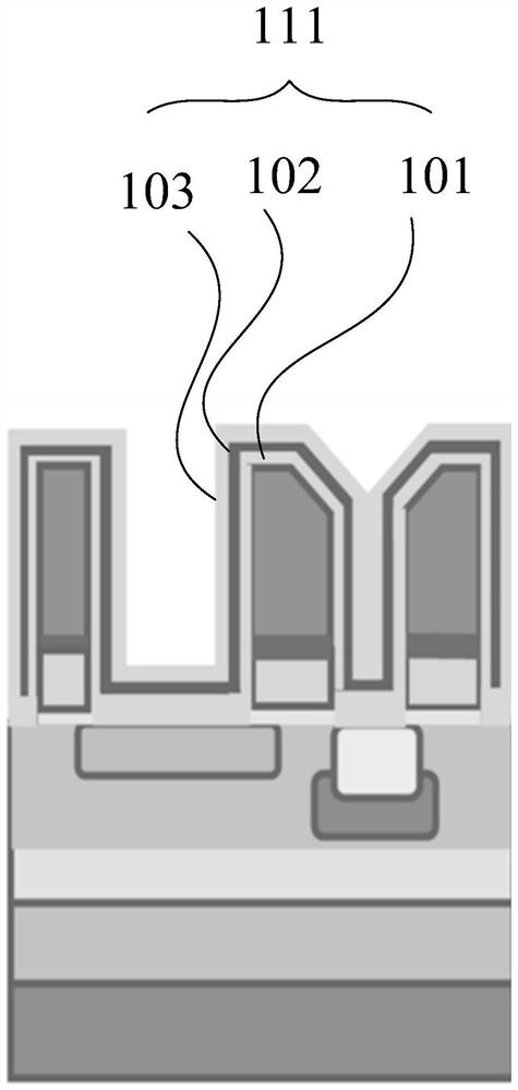
[0032] Step S301 is deposited to form an ONO layer of the side wall. The ONO layer includes a first oxide layer 101, a nitride layer 102, and a second oxide layer 103.
[0033] Step S302, wet etching to remove part of the second oxide layer.
[0034] Step S303, the ONO layer is carried out to form a side wall.
[0035] Then, other structures forming the or non-flash memory device, for example, the source drain ion implantation is performed on the storage unit area, and the source canal ion implantation is performed.
[0036] In the specific implementation, first, according to step S301, reference image 3 The first oxide layer 101, the nitride layer 102, and the second oxide layer 103 are formed, thereby for...
PUM
 Abstract
Description
Claims
Application Information
 - R&D
- Intellectual Property
- Life Sciences
- Materials
- Tech Scout
- Unparalleled Data Quality
- Higher Quality Content
- 60% Fewer Hallucinations
Browse by: Latest US Patents, China's latest patents, Technical Efficacy Thesaurus, Application Domain, Technology Topic, Popular Technical Reports.
© 2025 PatSnap. All rights reserved.Legal|Privacy policy|Modern Slavery Act Transparency Statement|Sitemap|About US| Contact US: help@patsnap.com