Method and device for reducing wafer overlay deviation

A technology for overlaying deviation and wafers, which is applied in photoplate-making process exposure devices, microlithography exposure equipment, photo-engraving process of patterned surfaces, etc., can solve problems such as scrap wafers and deviations, avoid resource waste, reduce The effect of overlay bias

Pending Publication Date: 2022-03-18
SOI MICRO CO LTD +1
View PDF0 Cites 4 Cited by
  • Summary
  • Abstract
  • Description
  • Claims
  • Application Information

AI Technical Summary

Problems solved by technology

[0002] When the lithography machine performs zero-layer exposure on the silicon wafer (wafer), it needs to be grasped and conveyed by the mechanical arm. After exposure, the imaging position of the circuit diagram of the zero-layer pattern on the silicon wafer depends entirely on the mechanical transfer arm of the lithography machi...

Method used


Image

  • Method and device for reducing wafer overlay deviation
  • Method and device for reducing wafer overlay deviation
  • Method and device for reducing wafer overlay deviation

Examples


Embodiment Construction

[0039] In order to make the purpose, technical solution and advantages of the present application clearer, the implementation manners of the present application will be further described in detail below in conjunction with the accompanying drawings.

[0040] The "plurality" mentioned herein means two or more. "And / or" describes the association relationship of associated objects, indicating that there may be three types of relationships, for example, A and / or B may indicate: A exists alone, A and B exist simultaneously, and B exists independently. The character " / " generally indicates that the contextual objects are an "or" relationship.

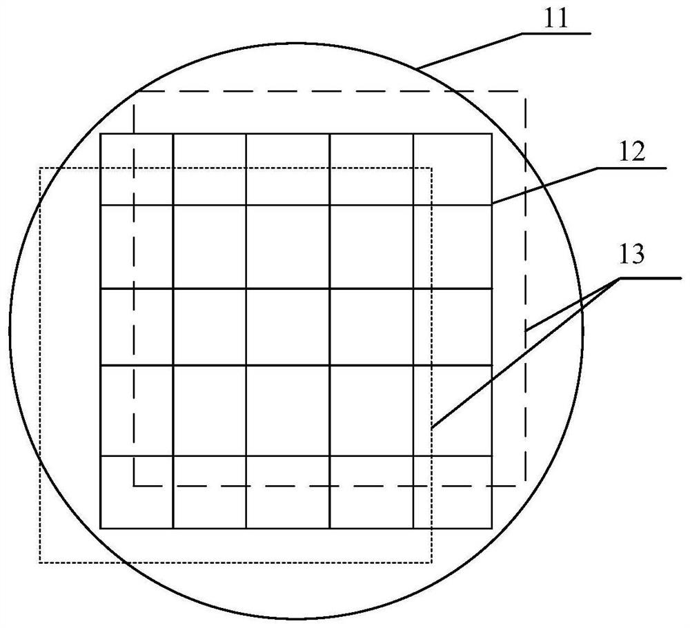
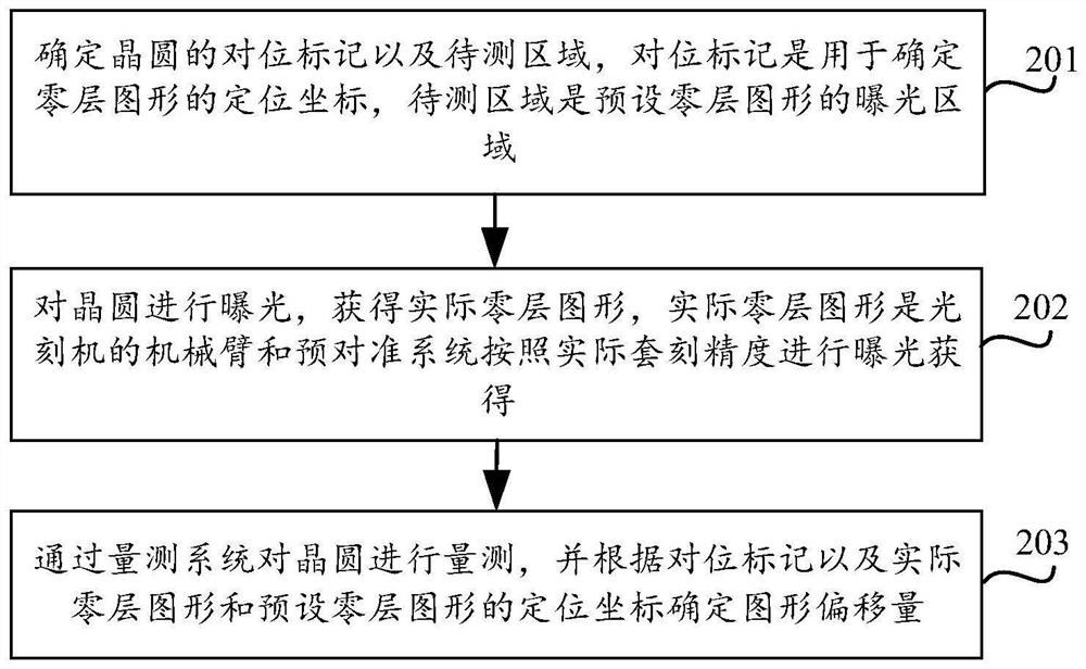
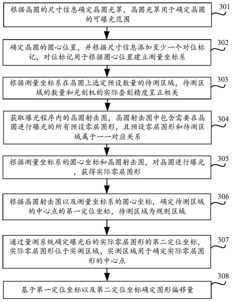
[0041] In related technologies, when a lithography machine performs zero-layer exposure on a wafer (silicon wafer), the imaging position of the circuit pattern on the wafer after exposure depends entirely on the precision of the mechanical transfer arm and the pre-alignment system of the lithography machine and The displacement accuracy of t...


PUM


Abstract

The embodiment of the invention discloses a method and device for reducing wafer overlay deviation, and the method comprises the steps: determining an alignment mark of a wafer and a to-be-detected region, the alignment mark being used for determining a positioning coordinate of a zero-layer pattern, and the to-be-detected region being an exposure region of a preset zero-layer pattern; exposing the wafer to obtain an actual zero-layer pattern; the wafer is measured through the measuring system, the pattern offset is determined according to the alignment mark and the positioning coordinates of the actual zero-layer pattern and the preset zero-layer pattern, and the pattern offset is used for calculating the alignment precision of the photoetching machine, so that when it is determined that the actual alignment precision of the photoetching machine is smaller than the alignment precision threshold value, response is made in time. According to the technical scheme, the alignment mark is arranged and the coordinate system is measured, so that the actual alignment precision of the photoetching machine can be determined according to the positioning coordinate of the zero-layer pattern, the wafer alignment deviation caused by the transmission deviation of the mechanical arm is corrected in time, and the resource waste is avoided.

Description

technical field [0001] The embodiments of the present application relate to the field of semiconductor technologies, and in particular to a method and device for reducing wafer overlay deviation. Background technique [0002] When the lithography machine performs zero-layer exposure on the silicon wafer (wafer), it needs to be grasped and conveyed by the mechanical arm. After exposure, the imaging position of the circuit diagram of the zero-layer pattern on the silicon wafer depends entirely on the mechanical transfer arm of the lithography machine and The accuracy of the pre-alignment system and the displacement accuracy of the loading platform. When the pre-alignment accuracy of the robotic arm exceeds the threshold due to maintenance or failure, it will cause a large deviation in the position of the circuit diagram exposed on the silicon wafer and the wafer will be scrapped. [0003] In the prior art, the current commonly used method in IC manufacturing is to select a few...

Claims


Application Information

Patent Timeline
IPC IPC(8): G03F7/20G03F9/00
CPCG03F7/70433G03F7/706G03F9/7088
Inventor 包晓明叶甜春朱纪军罗军李彬鸿赵杰
Owner SOI MICRO CO LTD
Why Eureka
Try Eureka