Display panel and display device
A display panel and flat technology, applied in the direction of semiconductor devices, electrical components, circuits, etc., can solve the problems of affecting the display effect, visual black area, blocking the light-emitting area, etc., so as to improve the display effect and reduce the effect of the upper black area.
- Summary
- Abstract
- Description
- Claims
- Application Information
AI Technical Summary
Problems solved by technology
Method used
Image

Examples
preparation example Construction
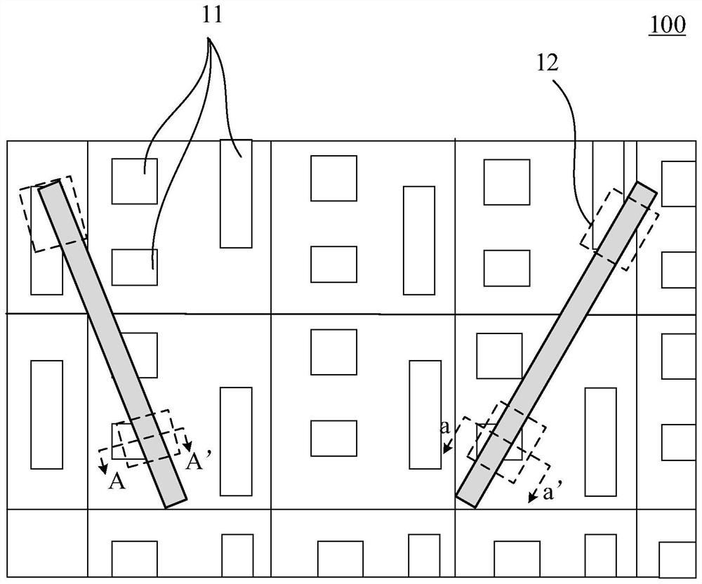
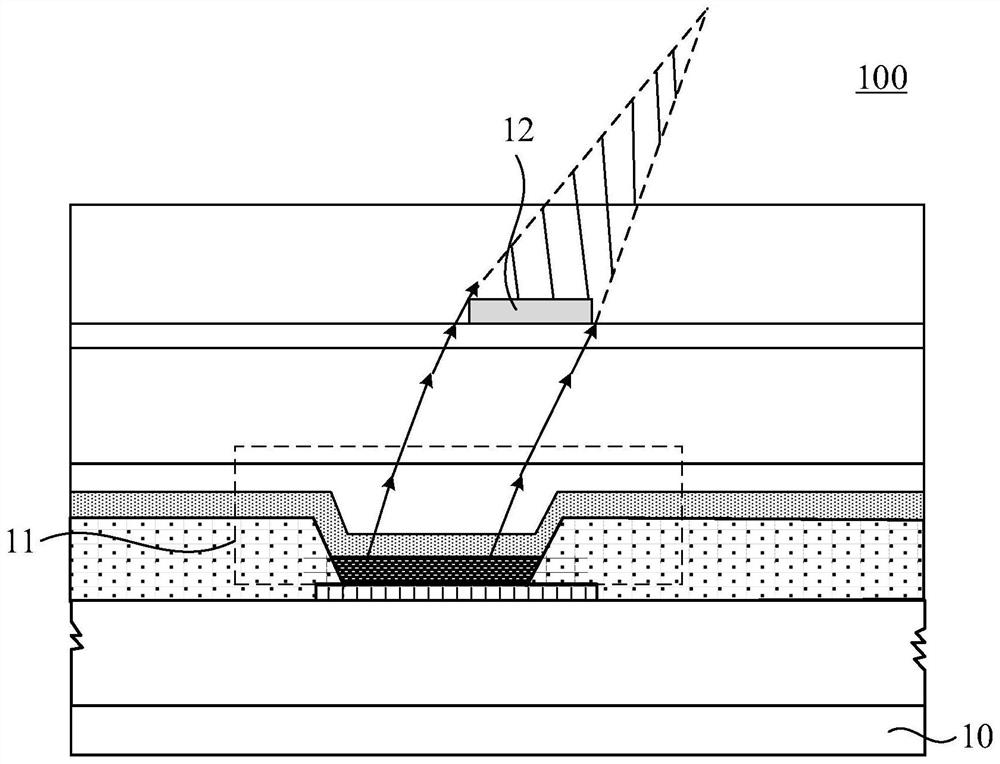
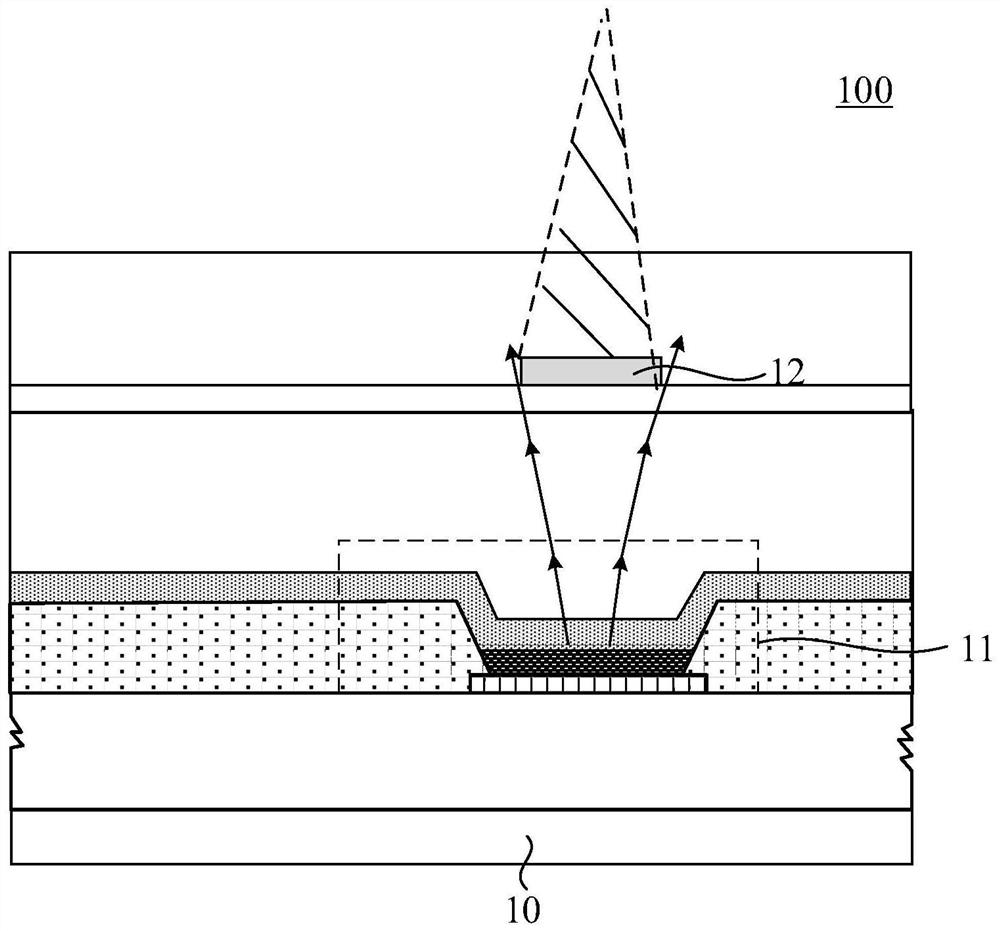
[0038] In the preparation of the display panel, due to the large number of light-shielding structures 40, it is unavoidable that the vertical projection (first projection) of the light-shielding structure 40 on the plane where the substrate 20 is located and the vertical projection (first projection) of the light-emitting element 30 on the plane where the substrate 20 is located ( The second projection) partially overlaps, combining Figure 4-Figure 6 or the vertical projection (first projection) of the light-shielding structure 40 on the plane where the substrate 20 is located and the vertical projection (second projection) of the light-emitting element 30 on the plane where the substrate 20 is located completely overlap, combined Figure 4 , Figure 7-Figure 14 As shown, these two structures cause visually there is a black area when viewing the display panel, corresponding to the position of the light-shielding structure 40 , thereby affecting the display effect. To solve t...
PUM
 Abstract
Description
Claims
Application Information