

Flip LED chip and manufacturing method thereof
A technology of LED chip and manufacturing method, which is applied in the direction of semiconductor devices, electrical components, circuits, etc., and can solve the problems such as large height difference of tin electrodes
- Summary
- Abstract
- Description
- Claims
- Application Information
AI Technical Summary
Problems solved by technology
Method used
Image

Examples
Embodiment 1
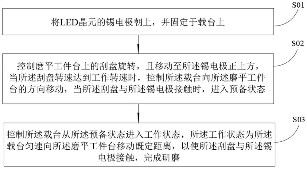
[0038] see figure 1 , figure 1 A method for fabricating a flip-chip LED chip proposed in Embodiment 1 of the present invention is shown, and the method specifically includes steps S01 to S03.
[0039] In step S01, the tin electrode of the LED wafer is turned upward and fixed on the stage.
[0040] It should be noted that when the LED wafer is fixed on the stage, the tin electrode should face upward, and at the same time, ensure that the LED wafer is relatively parallel to the scraper on the grinding workpiece table. When the scraper is in contact with the tin electrode, the rotating scraper will not make the LED chip shake, thus ensuring the grinding accuracy.
[0041] Step S02, control the scraper on the flattening workpiece table to rotate and move to just above the tin electrode, when the speed of the scraper reaches the working speed, control the carrier to move in the direction of the flattening workpiece table , when the scraper is in contact with the tin electrode, i...
Embodiment 2
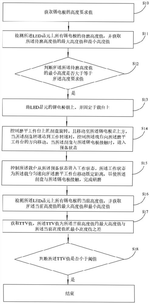
[0048]see figure 2 , figure 2 The manufacturing method of the flip-chip LED chip proposed in the second embodiment of the present invention is shown, and the method specifically includes steps S10 to S18.
[0049] In step S10, the height requirement value of the tin electrode is obtained.
[0050] It can be understood that the height requirement of the tin electrode is the target thickness of the tin electrode, and the target thickness of the tin electrode is also different according to different chips.
[0051] Step S11: Detect the height values to be ground of all the tin electrodes on the LED wafer, and obtain the maximum height value and the minimum height value of the height values to be ground.
[0052] It should be noted that after the tin brushing process is performed on the LED wafer, the height of the tin electrode is 15 μm to 150 μm. Due to the limitations of the tin brushing process, the height of the tin electrode will be uneven. If the height of the tin e...
Embodiment 3
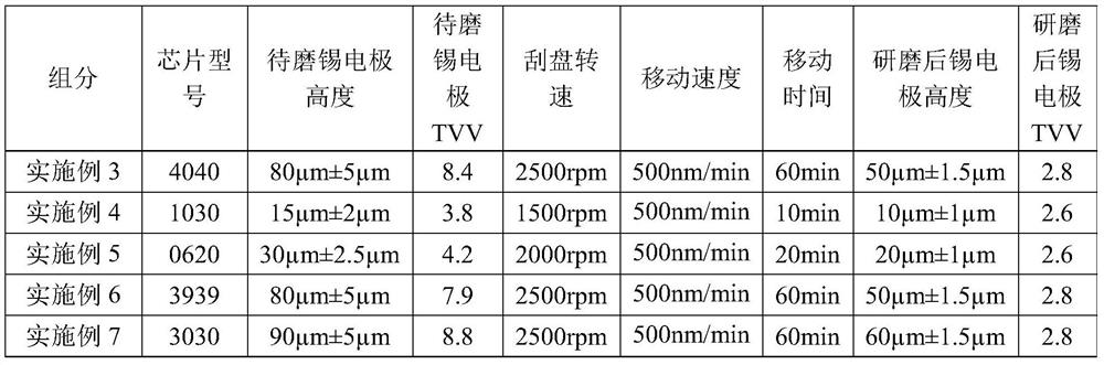
[0063] The manufacturing method of the flip-chip LED chip in this embodiment includes the following steps:
[0064] The LED wafer is placed on the carrier, and the vacuum generator is turned on, and then the LED wafer is adsorbed on the carrier. The chip type on the LED wafer is 4040 chip, and the height of the tin electrode on the 4040 chip is controlled to 80μm ±5μm, the actual TVV is 8.4, control the rotation of the scraper on the grinding workpiece table, and move it to the top of the tin electrode. When the speed of the scraper reaches 2500rpm, the stage moves up slowly until it contacts with the highest tin electrode Stop the movement, and then move up at a speed of 500nm / min for 60min. After 60min, the stage is reset, the height of the tin electrode is ground to 50μm±1.5μm, and the TTV is 2.8.
PUM
| Property | Measurement | Unit |
|---|---|---|
| height | aaaaa | aaaaa |
Abstract
Description
Claims
Application Information